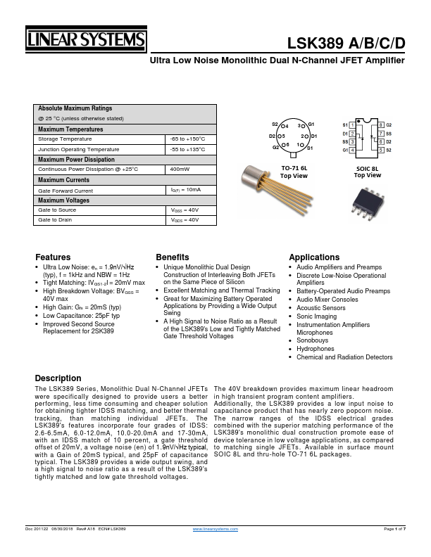
The LSK389 Series, Monolithic Dual N-Channel JFETs were specifically designed to provide users a better performing, less time consuming and cheaper solution for obtaining tighter IDSS matching, and better thermal tracking, than matching individual JFETs.
Key Features
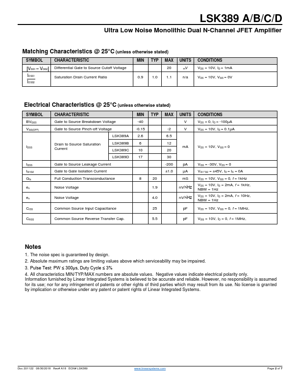
Ultra Low Noise: en = 1.9nV/√Hz (typ), f = 1kHz and NBW = 1Hz.
Tight Matching: IVGS1-2I = 20mV max.
High Breakdown Voltage: BVGSS =
40V max.
High Gain: Gfs = 20mS (typ).
Low Capacitance: 25pF typ.
Improved Second Source
Replacement for 2SK389
Benefits.
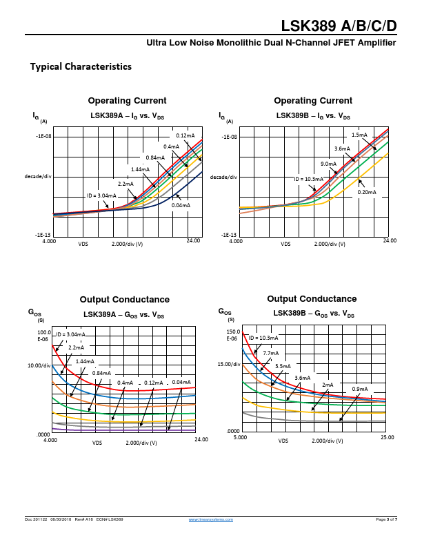
Unique Monolithic Dual Design Construction of Interleaving Both JFETs on the Same Piece of Silicon.
Full PDF Text Transcription for LSK389 (Reference)
Note: Below is a high-fidelity text extraction (approx. 800 characters) for
LSK389. For precise diagrams, and layout, please refer to the original PDF.
LSK389 A/B/C/D Ultra Low Noise Monolithic Dual N-Channel JFET Amplifier Absolute Maximum Ratings @ 25 °C (unless otherwise stated) Maximum Temperatures Storage Temperatur...
View more extracted text
5 °C (unless otherwise stated) Maximum Temperatures Storage Temperature Junction Operating Temperature Maximum Power Dissipation Continuous Power Dissipation @ +25°C Maximum Currents Gate Forward Current Maximum Voltages Gate to Source Gate to Drain -65 to +150°C -55 to +135°C 400mW IG(F) = 10mA VGSS = 40V VGDS = 40V S2 4 D2 5 G2 6 3 G1 2 D1 1 S1 TO-71 6L Top View SOIC 8L Top View Features Ultra Low Noise: en = 1.