CS2N60 Description
BR2N60(CS2N60) N-CHANNEL MOSFET/N 沟道 MOS 晶体管 用途: 用于高功率 DC/DC 转换和功率开关。 Purpose: These devices are well suited for high efficiency switching DC/DC converters and switch mode power supplies.
CS2N60 is N-CHANNEL MOSFET manufactured by LZG.
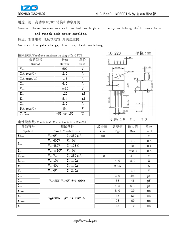
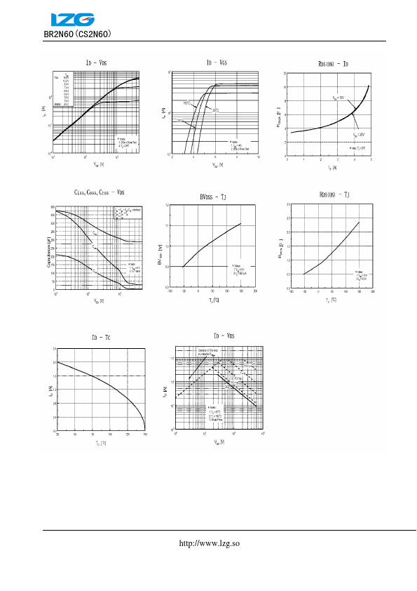
BR2N60(CS2N60) N-CHANNEL MOSFET/N 沟道 MOS 晶体管 用途: 用于高功率 DC/DC 转换和功率开关。 Purpose: These devices are well suited for high efficiency switching DC/DC converters and switch mode power supplies.