Download LTC3406B-2 Datasheet PDF
LTC3406B-2 page 2
Page 2
LTC3406B-2 page 3
Page 3

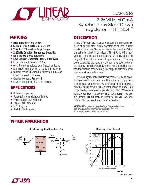
LTC3406B-2 Key Features

  • High Efficiency: Up to 96%
  • 600mA Output Current at VIN = 3V
  • 2.5V to 5.5V Input Voltage Range
  • 2.25MHz Constant Frequency Operation
  • No Schottky Diode Required
  • Low Dropout Operation: 100% Duty Cycle
  • Low Quiescent Current: 350µA
  • 0.6V Reference Allows Low Output Voltages
  • Shutdown Mode Draws < 1µA Supply Current
  • Current Mode Operation for Excellent Line and

LTC3406B-2 Description

U.

LTC3406B-2 Applications

  • 0.3V to 6V RUN, VFB Voltages
  • 0.3V to VIN SW Voltage (DC)
  • 0.3V to (VIN + 0.3V) P-Channel Switch Source Current (DC) ............. 800mA N-Channel Switch Sink Current (DC) ................. 800mA Peak SW Sink and Source
  • 40°C to 85°C Maximum Junction Temperature (Notes 3, 6) ..... 125°C Storage Temperature Range
  • 65°C to 150°C Lead Temperature (Soldering, 10 sec)................. 300°C