LTC6957-1 Key Features
- LVPECL
LTC6957-1 is Dual Output Buffer/Driver/Logic Converter manufactured by Linear Technology.
| Part Number | Description |
|---|---|
| LTC6957-2 | Dual Output Buffer/Driver/Logic Converter |
| LTC6957-3 | Dual Output Buffer/Driver/Logic Converter |
| LTC6957-4 | Dual Output Buffer/Driver/Logic Converter |
| LTC6910-1 | (LTC6910-1/-2/-3) Digitally Controlled Programmable Gain Amplifiers |
| LTC6910-2 | (LTC6910-1/-2/-3) Digitally Controlled Programmable Gain Amplifiers |
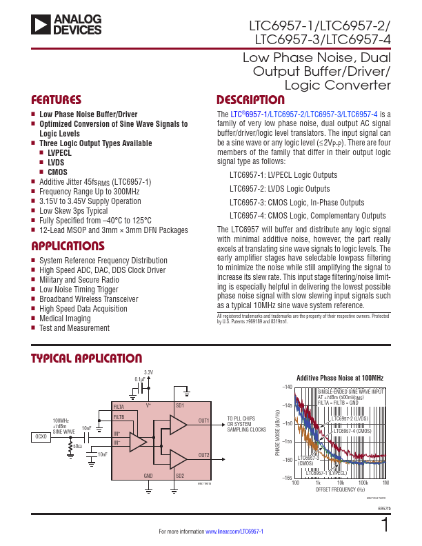
The LTC®6957-1/LTC6957-2/LTC6957-3/LTC6957-4 is a family of very low phase noise, dual output AC signal buffer/driver/logic level translators. The input signal can be a sine wave or any logic level (≤2VP-P). There are four members of the family that differ in their output logic signal type as follows:.