LTC1742 Overview
Key Features
- Ultralow jitter of 0.15psRMS allows undersampling of IF frequencies with excellent noise performance
- DC specs include ±3LSB INL and ±1LSB DNL
- The digital interface is compatible with 5V, 3V, 2V and LVDS logic levels
- The ENC and ENC inputs may be driven differentially from PECL, GTL and other low swing logic families or from single-ended TTL or CMOS
- The low noise, high gain ENC and ENC inputs may also be driven by a sinusoidal signal without degrading performance
- A separate output power supply can be operated from 0.5V to 5V, making it easy to connect directly to low voltage DSPs or FIFOs
- The TSSOP package with a flow-through pinout simplifies the board layout
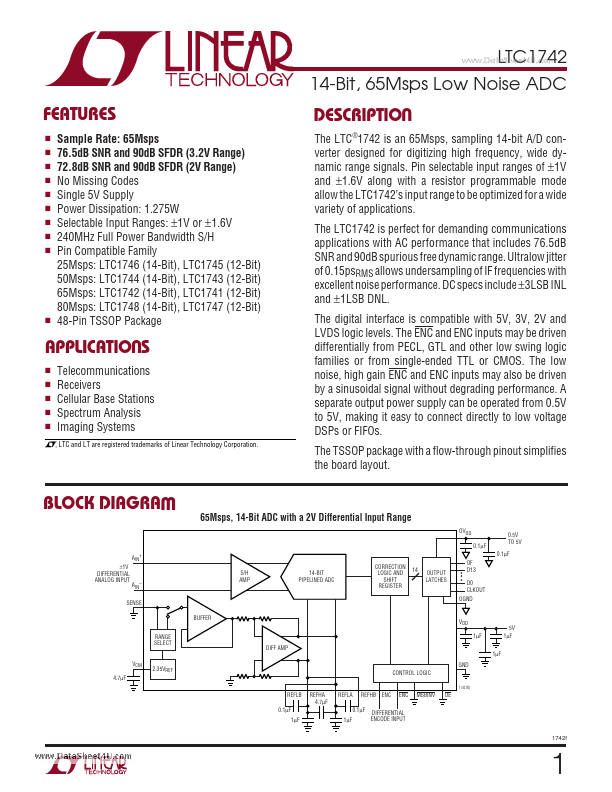
- BLOCK DIAGRA AIN+ ±1V DIFFERENTIAL ANALOG INPUT 65Msps, 14-Bit ADC with a 2V Differential Input Range OVDD 0.1µF OF D13 D0 CLKOUT 0.5V TO 5V