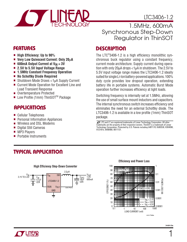
LTC3406-1.2 Description
U.
LTC3406-1.2 Key Features
- High Efficiency: Up to 90%
- Very Low Quiescent Current: Only 20µA
- 600mA Output Current at VIN = 3V
- 2.5V to 5.5V Input Voltage Range
- 1.5MHz Constant Frequency Operation
- No Schottky Diode Required
- Shutdown Mode Draws < 1µA Supply Current
- Current Mode Operation for Excellent Line and
- Overtemperature Protected
- Low Profile (1mm) ThinSOTTM Package
LTC3406-1.2 Applications
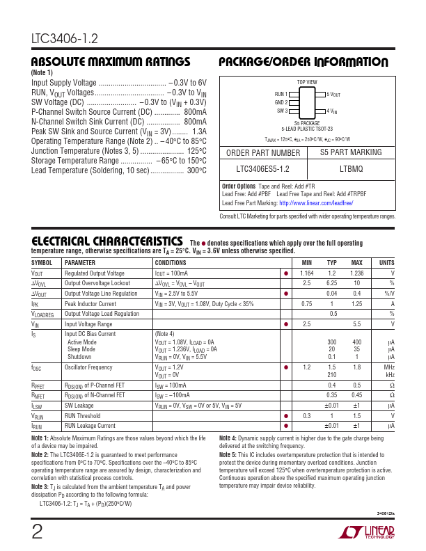
- 0.3V to 6V RUN, VOUT Voltages
- 0.3V to VIN SW Voltage (DC)
- 0.3V to (VIN + 0.3V) P-Channel Switch Source Current (DC) ............. 800mA N-Channel Switch Sink Current (DC) ................. 800mA Peak SW Sink and Source
- 40°C to 85°C Junction Temperature (Notes 3, 5) ...................... 125°C Storage Temperature Range
- 65°C to 150°C Lead Temperature (Soldering, 10 sec)................. 300°C