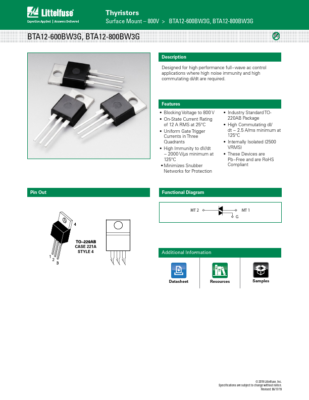
Thyristors
Surface Mount – 800V > BTA12-600BW3G, BTA12-800BW3G
Maximum Ratings (TJ = 25°C unless otherwise noted)
Rating
Symbol
Value
Unit
Peak Repetitive Off-State Voltage (Note 1)
BTA12−600BW3G
VDRM,
600
(Gate Open, Sine Wave 50 to 60 Hz, TJ = -40° to 125°C)
BTA12−800BW3G
VRRM
800
V
On-State RMS Current (Full Cycle Sine Wave, 60 Hz, TC = 80°C)
IT (RMS)
12
A
Peak Non-Repetitive Surge Current
(One Full Cycle Sine Wave, 60 Hz, TC = 25°C)
ITSM
105
A
Circuit Fusing Consideration (t = 8.3 ms)
I2t
46
A²sec
Non−Repetitive Surge Peak Off−State Voltage (TJ = 25°C, t = 10ms)
VDSM/ VRSM
VDSM/ VRSM
+100
V
Peak Gate Current (TJ = 125°C, t = 20ms)
IGM
4.0
A
Peak Gate Power (Pulse Width ≤ 1.0 µs, TC = 80°C)
PG(AV)
20
W
Average Gate Power (TJ = 125°C)
PG(AV)
1.0
W
Operating Junction Temperature Range
TJ
-40 to +125
°C
Storage Temperature Range
Tstg
-40 to +125
°C
RMS Isolation Voltage (t = 300 ms, R.H. ≤ 30%, TA = 25°C)
Viso
2500
V
Stresses exceeding Maximum Ratings may damage the device. Maximum Ratings are stress ratings only. Functional operation above the Recommended Operating Conditions is not implied.
Extended exposure to stresses above the Recommended Operating Conditions may affect device reliability.
1. VDRM and VRRM for all types can be applied on a continuous basis. Ratings apply for zero or negative gate voltage; however, positive gate voltage shall not be applied concurrent with negative
potential on the anode. Blocking voltages shall not be tested with a constant current source such that the voltage ratings of the devices are exceeded.
Thermal Characteristics
Rating
Thermal Resistance,
Junction−to−Case (AC)
Junction−to−Ambient
Maximum Lead Temperature for Soldering Purposes, 1/8” from case for
10 seconds
Symbol
R8JC
R8JA
TL
Value
2.5
60
260
Unit
°C/W
°C
Electrical Characteristics - OFF (TJ = 25°C unless otherwise noted ; Electricals apply in both directions)
Peak Repetitive Blocking Current
(VD = VDRM = VRRM; Gate Open)
Characteristic
TJ = 25°C
TJ = 125°C
Symbol
IDRM,
IRRM
Min
-
-
Typ
Max
Unit
-
0.005
mA
-
2.0
Electrical Characteristics - ON (TJ = 25°C unless otherwise noted; Electricals apply in both directions)
Characteristic
Forward On-State Voltage (Note 2) (ITM = ±17 A Peak)
Gate Trigger Current (Continuous dc) (VD = 12 V, RL = 30 Ω)
Holding Current
(VD = 12 V, Gate Open, Initiating Current = ±100 mA)
Latching Current (VD = 24 V, IG = 42 mA)
Gate Trigger Voltage (VD = 12 V, RL = 30 Ω)
Gate Non−Trigger Voltage (TJ = 125°C)
2. Indicates Pulse Test: Pulse Width ≤ 2.0 ms, Duty Cycle ≤ 2%.
Symbol
Min
Typ
VTM
−
−
MT2(+), G(+)
2.0
−
MT2(+), G(−)
IGT
MT2(−), G(−)
2.0
−
2.0
−
IH
−
−
MT2(+), G(+)
−
−
MT2(+), G(−)
IL
MT2(−), G(−)
−
−
−
−
MT2(+), G(+)
0.5
−
MT2(+), G(−)
VGT
0.5
−
MT2(−), G(−)
0.5
−
MT2(+), G(+)
0.2
−
MT2(+), G(−)
VGD
0.2
−
MT2(−), G(−)
0.2
−
Max
1.55
50
50
50
50
70
80
70
1.7
1.1
1.1
−
−
−
Unit
V
mA
mA
mA
V
V
© 2019 Littelfuse, Inc.
Specifications are subject to change without notice.
Revised: 06/17/19