MORESEMI MSN0318W
N-Channel MOSFET
| Part No. | MSN0318W |
|---|---|
| Datasheet | MSN0318W Download |
| Manufacturer | MORESEMI |
| Description | N-Channel MOSFET |
| Buy | Stock & Price |
GENERAL FEATURES
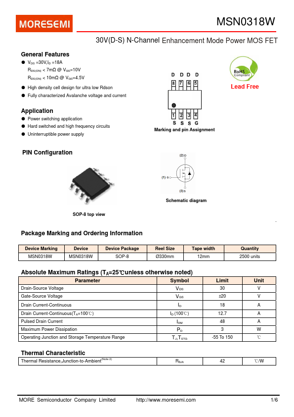
● VDS =30V,ID =18A RDS(ON) < 7mΩ @ VGS=10V RDS(ON) < 10mΩ @ VGS=4.5V● High density cell design for ultra low Rdson
● Fully characterized Avalanche voltage and current Lead Free Application
● Power switching application
● Hard switched and high frequency circuits
● Uninterruptible power supply Marking and pin Assignment PIN Configuration SOP-8 top view Schematic diagram Package Marking and Ordering Information Device Marking MSN0318W Device MSN0318W Device Package SOP-8 Reel Size Ø330mm Tape width 12mm Quantity 2500 units
ABSOLUTE MAXIMUM RATINGS
(TA=25℃unless otherwise noted) Parameter Symbol Drain-Source Voltage VDS Gate-Source Voltage VGS Drain Current-Continuous ID Drain Current-Continuous(TA=100℃) ID (100℃) Pulsed Drain Current Maximum Power Dissipation Operating Junction and Storage Temperature Range IDM PD TJ,TSTG Thermal Characteristic Thermal Resistan