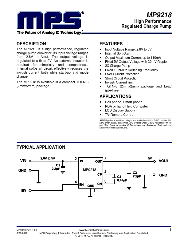
MP9218–HIGH PERFORMANCE REGULATED CHARGE PUMP
ORDERING INFORMATION
Part Number
MP9218DGT*
Package
TQFN-6(2mm*2mm)
Top Marking
See Below
* For Tape & Reel, add suffix –Z (e.g. MP9218DGT–Z)
For RoHS compliant packaging, add suffix –LF (e.g. MP9218DGT-LF-Z)
TOP MARKING
DE: product code of MP9218DGT;
Y: year code;
LLL: lot number;
PACKAGE REFERENCE
TOP VIEW
GND 1
6 EN
IN 2
5 CN
OUT 3
4 CP
TQFN-6 (2mm*2mm)
ABSOLUTE MAXIMUM RATINGS (1)
Supply Input Voltage.................. –0.3V to +6.0V
All Other Pins............................. –0.3V to +6.0V
Continuous Power Dissipation (TA = +25°C) (2)
……………………………………………....1.56W
Storage Temperature.............. –65°C to +150C
Junction Temperature ............................ +150C
Lead Temperature ................................. +260C
Recommended Operating Conditions (3)
Supply Voltage VIN ......................... 2.8V to 5.0V
Output Voltage VOUT....................................5.0V
Operating Junction Temp. (TJ). -40°C to +125°C
Thermal Resistance (4) θJA θJC
TQFN-6 (2mmx2mm)..............80 ...... 16 ...C/W
Notes:
1) Exceeding these ratings may damage the device.
2) The maximum allowable power dissipation is a function of
the maximum junction temperature TJ (MAX), the junction-
to-ambient thermal resistance θJA, and the ambient
temperature TA. The maximum allowable continuous
power dissipation at any ambient temperature is
calculated by PD (MAX) = (TJ (MAX)-TA)/θJA. Exceeding the
maximum allowable power dissipation will cause
excessive die temperature, and the regulator will go into
thermal shutdown. Internal thermal shutdown circuitry
protects the device from permanent damage.
3) The device is not guaranteed to function outside of its
operating conditions.
4) Measured on JESD51-7, 4-layer PCB.
MP9218 Rev. 1.01
www.MonolithicPower.com
2
8/23/2017
MPS Proprietary Information. Patent Protected. Unauthorized Photocopy and Duplication Prohibited.
© 2017 MPS. All Rights Reserved.