MX23L6410YC-10
MX23L6410YC-10 is 64M-BIT (8M x 8 / 4M x 16) Mask ROM manufactured by Macronix.
- Part of the MX23L6410 comparator family.
- Part of the MX23L6410 comparator family.
Features
- Bit organization
- 8M x 8 (byte mode)
- 4M x 16 (word mode)
- Fast access time
- Random access: 90ns (max.) for 3.0V~3.6V 100ns (max.) for 2.7V~3.6V Notes: die form: 2.7~3.6V 90ns
- Current
- Operating: 50mA (max.)
- Standby: 15uA (max.)
- Supply voltage
- 2.7V~3.6V
- Package
- 44 pin SOP (500 mil)
- 48 pin TSOP (12mm x 20mm)
- 44 pin TSOP (Type II)
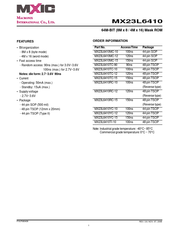
MX23L6410
64M-BIT (8M x 8 / 4M x 16) Mask ROM
ORDER INFORMATION
Part No. MX23L6410MC-10 MX23L6410MC-12 MX23L6410MC-15 MX23L6410TC-90 MX23L6410TC-10 MX23L6410TC-12 MX23L6410TC-15 MX23L6410RC-10
Access Time 100ns 120ns 150ns 90ns 100ns 120ns 150ns 100ns
MX23L6410RC-12
120ns
MX23L6410RC-15
150ns
MX23L6410YC-10 MX23L6410YC-12...