MAX5308
MAX5308 is Octal 10-Bit VoltageOutput DACs manufactured by Maxim Integrated.
Description
II. Manufacturing Information III. Packaging Information V. Quality Assurance Information VI. Reliability Evaluation IV. Die Information Attachments
I. Device Description
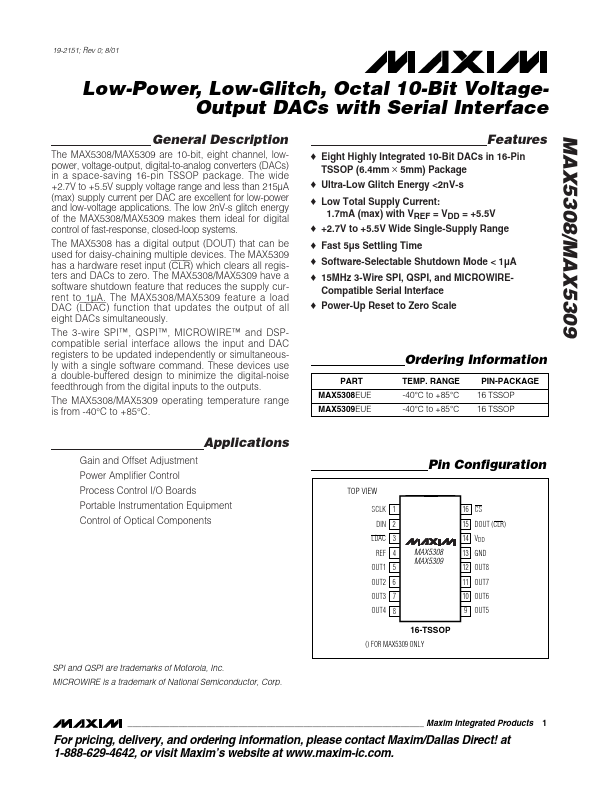
A. General The MAX5309 is a10-bit, eight channel, low-power, voltage-output, digital-to-analog converters (DAC) in a spacesaving 16-pin TSSOP package. The wide +2.7V to +5.5V supply voltage range and less than 215µA (max) supply current per DAC is excellent for low-power and low-voltage applications. The low 2n V-s glitch energy of the MAX5309 makes it ideal for digital control of fast-response, closed-loop systems. The MAX5309 has a hardware reset input (CLR-bar) which clears all registers and DACs to zero. The MAX5309 has a software shutdown feature that reduces the supply current to 1µA. The MAX5308 features a load DAC (LDAC-bar) function that updates the output of all eight DACs simultaneously. The 3-wire SPI™, QSPI™, MICROWIRE™ and DSP-patible serial interface allows the input and DAC registers to be updated independently or simultaneously with a single software mand. This device uses a double-buffered design to minimize the digital-noise feedthrough from the digital inputs to the outputs. The MAX5309 operating temperature range is from -40°C to +85°C
B. Absolute Maximum Ratings Item VDD to GND All Other Pins to GND Maximum Current Into Any Pin Operating Temperature Range Junction Temperature Storage Temperature Range Lead Temperature (soldering, 10s) Continuous Power Dissipation (TA = +70°C) 16-Pin TSSOP Derates above +70°C 16-Pin TSSOP
Rating -0.3V to +6V -0.3V to (VDD + 0.3V) ±50m A -40°C to +85°C +150°C -65°C to +150°C +300°C 775m W 9.4m W/°C
II. Manufacturing Information A. Description
/Function: B. Process: C. Number of Device Transistors: D. Fabrication Location: E. Assembly Location: F. Date of Initial Production: Low-Power, Low-Glitch, Octal 10-Bit Voltage-Output DACs with Serial Interface S6 (Standard 0.6 micron silicon gate CMOS)...