DS1644P Description
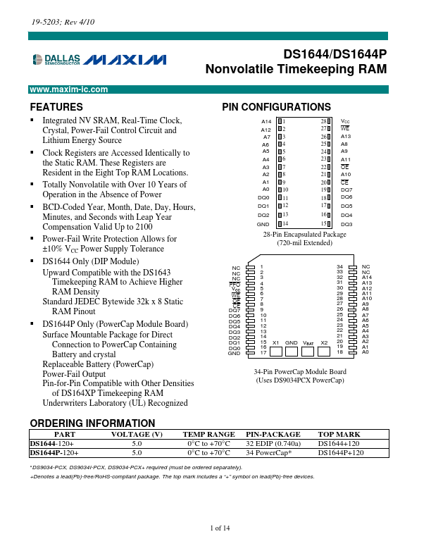
Requires a pull-up resistor for proper operation. No Connection Crystal Connection VBAT Battery Connection DESCRIPTION The DS1644 is a 32k x 8 nonvolatile static RAM with a full function real time clock, which are both accessible in a byte-wide format. The nonvolatile timekeeping RAM is functionally equivalent to any JEDEC standard 32k x 8 SRAM.
DS1644P Key Features
- Integrated NV SRAM, Real-Time Clock, Crystal, Power-Fail Control Circuit and Lithium Energy Source
- Clock Registers are Accessed Identically to the Static RAM. These Registers are Resident in the Eight Top RAM Locations
- Totally Nonvolatile with Over 10 Years of Operation in the Absence of Power
- BCD-Coded Year, Month, Date, Day, Hours, Minutes, and Seconds with Leap Year pensation Valid Up to 2100
- Power-Fail Write Protection Allows for ±10% VCC Power Supply Tolerance
- DS1644 Only (DIP Module)
- DS1644P Only (PowerCap Module Board)