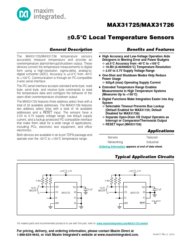
MAX31725/MAX31726
±0.5°C Local Temperature Sensors
ABSOLUTE MAXIMUM RATINGS
(All voltages relative to GND.)
Voltage Range on VDD, SDA, SCL, A0, A1.............-0.3V to +4V
Voltage Range on A2, RESET, OS............ -0.3V to (VDD + 0.3V)
Input Current at Any Pin .................................................... +5mA
Package Input Current .................................................... +20mA
Continuous Power Dissipation (TA = +70NC)
TDFN (derate 24.4mW/NC above +70NC)................1951.2mW
ESD Protection (All Pins, Human Body Model) (Note 1)..... Q4000V
Operating Temperature Range......................... -55NC to +150NC
Junction Temperature......................................................+150NC
Storage Temperature Range............................. -65NC to +150NC
Lead Temperature (soldering, 10s).................................+300NC
Soldering Temperature (reflow) ......................................+260NC
Note 1: Human Body Model, 100pF discharged through a 1.5kI resistor.
Stresses beyond those listed under “Absolute Maximum Ratings” may cause permanent damage to the device. These are stress ratings only, and functional opera-
tion of the device at these or any other conditions beyond those indicated in the operational sections of the specifications is not implied. Exposure to absolute
maximum rating conditions for extended periods may affect device reliability.
PACKAGE THERMAL CHARACTERISTICS (Note 2)
TDFN
Junction-to-Ambient Thermal Resistance (qJA)...........41°C/W
Junction-to-Case Thermal Resistance (qJC)..................8°C/W
Note 2: Package thermal resistances were obtained using the method described in JEDEC specification JESD51-7, using a four-layer
board. For detailed information on package thermal considerations, refer to www.maximintegrated.com/thermal-tutorial.
RECOMMENDED OPERATING CONDITIONS
(TA = -55NC to +150NC, unless otherwise noted.) (Notes 3, 4)
PARAMETER
SYMBOL
CONDITIONS
Operating Supply Voltage
Input High Voltage
Input Low Voltage
VDD
VIH
VIL
MIN TYP MAX
2.5 3.3 3.7
VDD x 0.7
VDD x 0.3
UNITS
V
V
V
ELECTRICAL CHARACTERISTICS
(VDD = 2.5V to 3.7V, TA = -55NC to +150NC, unless otherwise noted. Typical values are VDD = 3.3V, TA = +25NC.) (Note 3)
PARAMETER
SYMBOL
CONDITIONS
MIN TYP MAX
Accuracy (Note 5)
Temperature Conversion Noise
2.5V P + VDD P 3.7V, -40NC P TA P +105NC -0.5 ±0.1 +0.5
2.5V P + VDD P 3.7V, -55NC P TA P +150NC -0.7
+0.7
0.0625
Temperature Data Resolution
16 16
UNITS
NC
NC
Bits
Conversion Time
44 50
ms
First Conversion Completed
Quiescent Supply Current
Data ready after POR
I2C inactive, TA = -40NC to +125NC
Shutdown mode, I2C inactive, TA =
IDD
-40NC to +125NC
I2C inactive, TA = +150NC
Shutdown mode, I2C inactive,
TA = +150NC
50
600 925
2.5 3.5
800
4.2
ms
FA
Maxim Integrated
2