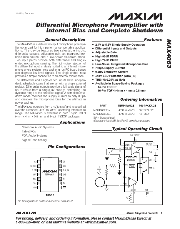
Differential Microphone Preamplifier with
Internal Bias and Complete Shutdown
ABSOLUTE MAXIMUM RATINGS
Supply Voltage (VCC to GND). .................................-0.3V to +6V
Any Other Pin to GND ................................-0.3V to (VCC + 0.3V)
Duration of Short Circuit to GND or VCC ....................Continuous
Continuous Input Current (any pin) ................................ ±10mA
Continuous Power Dissipation (TA = +70°C)
14-Pin TSSOP (derate 10.0mW/°C above +70°C) .....796.8mW
16-Pin TQFN (derate 25.0mW/°C above +70°C) ........2000mW
Operating Temperature Range ...........................-40°C to +85°C
Storage Temperature Range .............................-65°C to +150°C
Lead Temperature (soldering, 10s) .................................+300°C
Soldering Temperature (reflow) .......................................+260°C
Stresses beyond those listed under “Absolute Maximum Ratings” may cause permanent damage to the device. These are stress ratings only, and functional
operation of the device at these or any other conditions beyond those indicated in the operational sections of the specifications is not implied. Exposure to
absolute maximum rating conditions for extended periods may affect device reliability.
ELECTRICAL CHARACTERISTICS
(VCC = 3V, VGND = 0V, VSHDN = VCC, VINT/AUX = 0V, RG = 11.11kΩ, RL = 100kΩ to 1.5V, RBIAS = ∞, VOUT is measured between
OUT and OUT. TA = TMIN to TMAX, unless otherwise noted. Typical values are at TA = +25°C.) (Notes 1 and 2)
PARAMETER
SYMBOL
CONDITIONS
Supply Voltage Range
VCC Inferred from PSRR test
Supply Current
ICC
Output Common-Mode Voltage
VOCM
Slew Rate
SR AV = 20V/V
Supply Current in Shutdown
ISHDN VSHDN = 0V
Output Short-Circuit Current
To GND
ISC
To VCC
DIFFERENTIAL INPUT (VINT/AUX = 0V)
Input Offset Voltage
VOS TA = +25°C
Common-Mode Input Voltage Range VCM Inferred from CMRR test
Maximum Differential Input Voltage VDIFFMAX AV = 2V/V
Small-Signal Bandwidth
BW-3dB
Input Resistance
RIN Either differential input
Input Resistance Match
RMATCH
Input Noise-Voltage Density
en
AV = 20V/V, f = 1kHz
AV = 200V/V, f = 1kHz
RMS Output Noise Voltage
VNRMS AV = 20V/V, BW = 22Hz to 22kHz
Total Harmonic Distortion Plus Noise
THD+N
AV = 20V/V, f = 1kHz, VOUT = 0.7VRMS,
BW = 22Hz to 22kHz
Differential Gain
Common-Mode Rejection Ratio
Power-Supply Rejection Ratio
AVDIFF
CMRR
PSRR
1V < VCM < 2V,
VOUT = 0.7VRMS
RG = open
RG = 11.11kΩ
RG = 1.01kΩ
VCM = 500mVP-P, f = 1kHz
TA = +25°C
TA = TMIN - TMAX
VCC = 5V ±100mV, f = 1kHz
MIN TYP
2.4
0.75
1.25 1.5
±1
0.001
30
30
MAX
5.5
1.1
1.75
1
UNITS
V
mA
V
V/µs
µA
mA
±1
1
1
600
100
1
70
12
225
0.05
2
19.2 20
200
70
95
85
86
mV
2V
V
kHz
kΩ
%
nV/√Hz
µVRMS
%
20.8 V/V
dB
dB
2 _______________________________________________________________________________________