MAX44290
1.8V, 15MHz, Low-Offset, Low-Power,
Rail-to-Rail I/O Op-Amp
General Description
The MAX44290 offers a unique combination of high-
speed, precision, and low-voltage operation, making them
ideally suited for a large number of signal-processing
functions, such as filtering and amplification of signals in
portable and industrial equipment.
This amplifier features an input offset of less than 50µV
and a high-gain bandwidth product of 15MHz while
maintaining a low 1.8V supply rail. The devices’ rail-to-
rail input/outputs and low noise guarantee maximum
dynamic range in demanding applications, such as 12-to-
14-bit SAR ADC drivers. Unlike traditional rail-to-rail input
structures, input crossover distortion is absent due to an
optimized input stage with an ultra-quiet charge pump.
The device includes a fast-power-on shutdown mode for
further power savings. The operational amplifier operates
from a supply range of 1.8V to 5.5V over -40°C to 125°C
temperature range, and can operate down to 1.7V over
the 0 to 70°C temperature range. It is available in a tiny,
6-bump wafer-level package (WLP), with 0.4mm-pitch.
Ordering Information appears at end of data sheet.
Benefits and Features
●● Low 1.8V Supply Rail Over the -40°C to +125°C
Range
●● 1.7V Supply Rail Over 0°C to 70°C Range
●● 15MHz Unity-Gain Bandwidth
●● Low 12.7nV/√Hz Input Voltage-Noise Density
●● Low 50µV (max) Input Offset Voltage at +25°C
●● 500fA Low Input Bias Current
●● 750µA Quiescent Current
●● < 1µA Supply Current in Shutdown
●● Low 105dB Total Harmonic Distortion
Applications
●● Notebooks
●● 3G/4G Handsets
●● Portable Medical Instruments
●● Battery-Operated Devices
●● Analog-to-Digital Converter Buffers
●● Transimpedance Amplifiers
●● General-Purpose Signal Processing
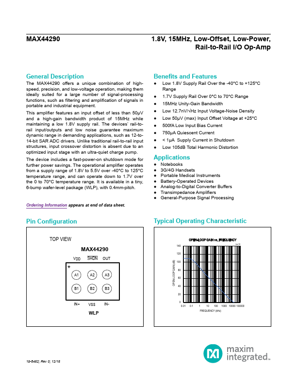
Pin Configuration
Typical Operating Characteristic
TOP VIEW
MAX44290
VDD SHDN OUT
A1 A2 A3
B1 B2 B3
IN+ VSS IN-
WLP
OPEN-LOOP GAIN vs. FREQUENCY
140 toc10
120
100
80
60
40
20
0
0.01 0.1
1 10 100 1000 10000 100000
FREQUENCY (kHz)
19-8452; Rev 0; 12/15