48L256
48L256 is 256-Kbit SPI Serial EERAM manufactured by Microchip Technology.
256-Kbit SPI Serial EERAM
Serial SRAM Features
- Unlimited Reads/Unlimited Writes:
- Standard serial SRAM protocol
- Symmetrical timing for reads and writes
- SRAM Array:
- 32,768 x 8 bit
- High-Speed SPI Interface:
- Up to 66 MHz
- Schmitt Trigger inputs for noise suppression
- Low-Power CMOS Technology:
- Active current: 5 m A (maximum)
- Standby current: 300 μA (at 85°C maximum)
- Hibernate current: 3 μA (at 85°C maximum)
Hidden EEPROM Backup Features
- Cell-Based Nonvolatile Backup:
- Mirrors SRAM array cell-for-cell
- Transfers all data to/from SRAM cells in parallel (all cells at same time)
- Invisible-to-User Data Transfers:
- VCC level monitored inside device
- SRAM automatically saved on power disrupt
- SRAM automatically restored on VCC return
- 100,000 Backups Minimum (at 85°C)
- 100 Years Retention (at 55°C)
Other Features of the 48L256
- Operating Voltage Range: 2.7V-3.6V
- Temperature Ranges:
- Industrial (I): -40°C to +85°C
- ESD Protection: >2,000V
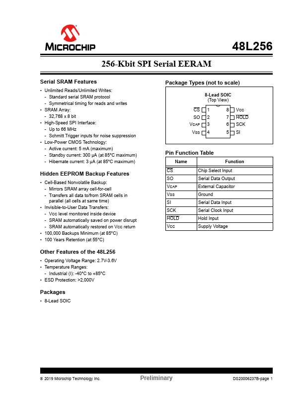
Packages...