Microchip Technology ATmega4809
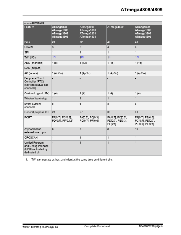
the ATmega4809 is using the die of the 48-pin ATmega4809 but offers fewer connected pads. For this reason, the pins PB[5:0] and PC[7:6] must be disabled (INPUT_DISABLE) or enable pull-ups (PULLUPEN). The name of a device in the megaAVR 0-series is decoded as follows: © 2021 Microchip Technology Inc.| Part No. | ATmega4809 |
|---|---|
| Datasheet | ATmega4809 Download |
| Manufacturer |  Microchip Technology |
| Description | Microcontrollers |
| Buy | Stock & Price |

FEATURES
● AVR® CPU: – Single-cycle I/O access – Two-level interrupt controller – Two-cycle hardware multiplier● Memories: – 48 KB In-system self-programmable Flash memory – 256B EEPROM – 6 KB SRAM – Write/Erase endurance:
● Flash 10,000 cycles
● EEPROM 100,000 cycles – Data retention: 40 years at 55°C
● System: – Power-on Reset (POR) circuit – Brown-out Detector (BOD) – Clock options:
● 16/20 MHz low-power internal oscillator
● 32.768 kHz Ultra Low-Power (ULP) internal oscillator
● 32.768 kHz external crystal oscillator
● External clock input – Single-pin Unified Program Debug Interface (UPDI) – Three sleep modes:
● Idle with all peripherals running for immediate wake-up
● Standby – Configurable operation of selected peripherals – SleepWalking peripherals
● Power-Down with lim