MT28F322D20
Overview
- Flexible dual-bank architecture - Support for true concurrent operation with zero latency - Read bank a during program bank b and vice versa - Read bank a during erase bank b and vice versa
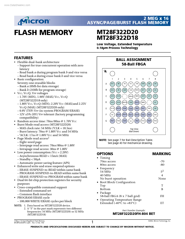
- Basic configuration: Seventy-one erasable blocks - Bank a (8Mb for data storage) - Bank b (24Mb for program storage)
- VCC, VCCQ, VPP voltages - 1.70V (MIN), 1.90V (MAX) VCC, VCCQ (MT28F322D18 only) - 1.80V VCC, VCCQ (MIN); 2.20V VCC (MAX)and 2.25V VCCQ (MAX) (MT28F322D20 only) - 0.9V (TYP) VPP (in-system PROGRAM/ERASE) - 12V ±5% (HV) VPP tolerant (factory programming compatibility)
- Random access time: 70ns/80ns @ 1.70V VCC
- Burst Mode read access (MT28F322D20) - MAX clock rate: 54 MHz (tCLK = 18.5ns) - Burst latency: 70ns @ 1.80V VCC and 54 MHz - tACLK: 17ns @ 1.80V VCC and 54 MHz
- Page Mode read access1 - Eight-word page - Interpage read access: 70ns/80ns @ 1.80V - Intrapage read access: 30ns @ 1.80V
- Low power consumption (VCC = 2.20V) - Asynchronous READ < 15mA (MAX) - Standby < 50µA - Automatic power saving feature (APS)
- Enhanced write and erase suspend options - ERASE-SUSPEND-to-READ within same bank - PROGRAM-SUSPEND-to-READ within same bank - ERASE-SUSPEND-to-PROGRAM within same bank
- Dual 64-bit chip protection registers for security purposes
- Cross-compatible command support - Extended command set - Common flash interface