APT20M18B2VFR
APT20M18B2VFR A20M18LVFR
200V 100A 0.018Ω
POWER MOS V® FREDFET
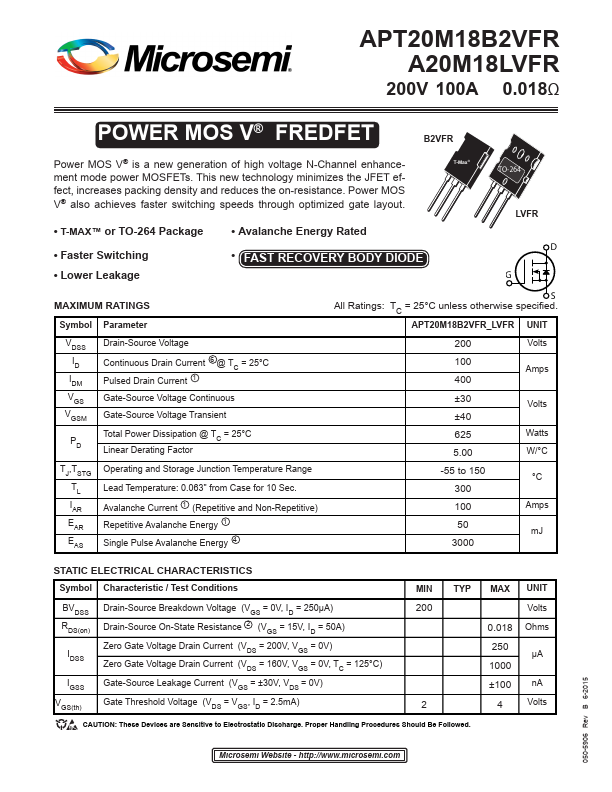
B2VFR
Power MOS V® is a new generation of high voltage N-Channel enhancement mode power MOSFETs. This new technology minimizes the JFET effect, increases packing density and reduces the on-resistance. Power MOS V® also achieves faster switching speeds through optimized gate layout.
T-Max®
TO-264
LVFR
- T-MAX™ or TO-264 Package
- Avalanche Energy Rated
- Faster Switching
- FAST RECOVERY BODY DIODE
- Lower Leakage
MAXIMUM RATINGS
Symbol Parameter
VDSS ID IDM VGS
VGSM
Drain-Source Voltage Continuous Drain Current 6 @ TC = 25°C Pulsed Drain Current 1 Gate-Source Voltage Continuous Gate-Source Voltage Transient
Total Power Dissipation @ TC = 25°C Linear Derating Factor
TJ,TSTG TL IAR EAR EAS
Operating and Storage Junction Temperature Range
Lead Temperature: 0.063" from Case for 10 Sec. Avalanche Current 1 (Repetitive and Non-Repetitive) Repetitive Avalanche Energy 1 Single Pulse Avalanche Energy...