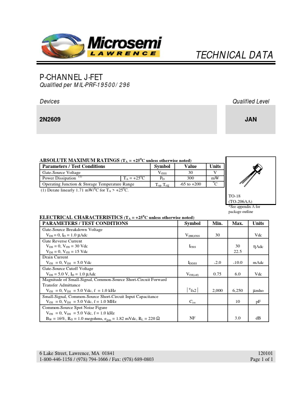
Click to expand full text
TECHNICAL DATA
P-CHANNEL J-FET
Qualified per MIL-PRF-19500/296 Devices 2N2609 Qualified Level JAN
ABSOLUTE MAXIMUM RATINGS (TA = +250C unless otherwise noted) Parameters / Test Conditions Symbol Value
Gate-Source Voltage Power Dissipation (1) TA = +250C Operating Junction & Storage Temperature Range (1) Derate linearly 1.71 mW/0C for TA > +250C. VGSS PD Top, Tstg 30 300 -65 to +200
Units
V mW 0 C TO-18 (TO-206AA)
*See appendix A for package outline
ELECTRICAL CHARACTERISTICS (TA = +250C unless otherwise noted) PARAMETERS / TEST CONDITIONS Symbol
Gate-Source Breakdown Voltage VDS = 0, IG = 1.0 µAdc Gate Reverse Current VDS = 0, VGS = 30 Vdc VDS = 0, VGS = 15 Vdc Drain Current VGS = 0, VDS = 5.0 Vdc Gate-Source Cutoff Voltage VDS = 5.0 V, ID = 1.