J202
J202 is Amplifier manufactured by Micross.
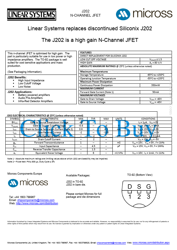
J202 N-CHANNEL JFET
Linear Systems replaces discontinued Siliconix J202 The J202 is a high gain N-Channel JFET
This n-channel JFET is optimised for high gain. The part is particularly suitable for use in low power or high impedance amplifiers. The TO-92 package is well suited for cost sensitive applications and mass production. (See Packaging Information). Features
DIRECT REPLACEMENT FOR SILICONIX J202 LOW CUT OFF VOLTAGE VGS(off) ≤ 1.5 HIGH GAIN AV = 80 V/V ABSOLUTE MAXIMUM RATINGS @ 25°C (unless otherwise noted) Maximum Temperatures Storage Temperature Operating Junction Temperature Maximum Power Dissipation Continuous Power Dissipation MAXIMUM CURRENT Forward Gate Current (Note 1) MAXIMUM VOLTAGES Gate to Drain Voltage Gate to Source Voltage ‐65°C to +150°C ‐55°C to +135°C 350m W 50m A VGDS = ‐40V VGSS = ‐40V
..
J202 Benefits:
- -
- -
- - High Input Impedance Low Cutoff Voltage Low Noise Battery powered amplifiers Audio Pre-Amplifiers Infra-Red Detector Amplifiers
J202 Applications:
J202 ELECTRICAL CHARACTERISTICS @ 25°C (unless otherwise noted) SYMBOL CHARACTERISTIC MIN BVGSS Gate to Source Breakdown Voltage ‐40 VGS(off) Gate to Source Cutoff Voltage ‐0.8 IDSS Drain to Source Saturation Current (Note 2) 0.9 IGSS Gate Reverse Current ‐2 IG Gate Operating Current ‐‐ ID(off) Drain Cutoff Current ‐‐ gfs Forward Transconductance 1 Ciss Input Capacitance ‐‐ Crss Reverse Transfer Capacitance ‐‐ en Equivalent Noise Voltage ‐‐
Click To Buy
V m A p A m S p F n V/√Hz Available Packages: J202 in TO-92 J202 in bare die. Please contact Micross for full package and die dimensions TO-92 (Bottom View)
TYP. ‐‐ ‐‐ ‐‐ ‐‐ ‐2 2 ‐‐ 4.5 1.3 6
MAX ‐‐ ‐4 4.5 ‐100 ‐‐ ‐‐ ‐‐ ‐‐ ‐‐ ‐‐
UNITS
CONDITIONS IG = 1µA, VDS = 0V VDS = 15V, ID = 10n A VDS = 15V, VGS = 0V VGS = ‐20V, VDS = 0V VDG = 10V, ID = 0.1m A VDS = 15V, VGS = ‐5V VDS = 15V, VGS = 0V , f = 1k Hz ...