J309
J309 is Amplifier manufactured by Micross.
J309 N-CHANNEL JFET
Linear Systems replaces discontinued Siliconix J309
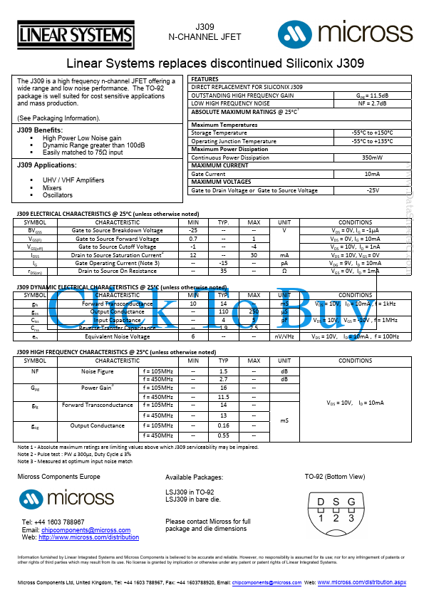
The J309 is a high frequency n-channel JFET offering a wide range and low noise performance. The TO-92 package is well suited for cost sensitive applications and mass production. (See Packaging Information). Features
DIRECT REPLACEMENT FOR SILICONIX J309 OUTSTANDING HIGH FREQUENCY GAIN LOW HIGH FREQUENCY NOISE ABSOLUTE MAXIMUM RATINGS @ 25°C1 Gpg = 11.5d B NF = 2.7d B
Maximum Temperatures Storage Temperature ‐55°C to +150°C
- High Power Low Noise gain Operating Junction Temperature ‐55°C to +135°C
- Dynamic Range greater than 100d B Maximum Power Dissipation
- Easily matched to 75Ω input Continuous Power Dissipation 350m W J309 Applications: MAXIMUM CURRENT Gate Current 10m A
- UHV / VHF Amplifiers MAXIMUM VOLTAGES
- Mixers Gate to Drain Voltage or Gate to Source Voltage ‐25V
- Oscillators J309 ELECTRICAL CHARACTERISTICS @ 25°C (unless otherwise noted) SYMBOL CHARACTERISTIC MIN TYP. MAX UNIT CONDITIONS BVGSS Gate to Source Breakdown Voltage ‐25 ‐‐ ‐‐ V VDS = 0V, IG = ‐1µA VGS(F) Gate to Source Forward Voltage 0.7 ‐‐ 1 VDS = 0V, IG = 10m A VGS(off) Gate to Source Cutoff Voltage ‐1 ‐‐ ‐4 VDS = 10V, ID = 1n A IDSS Drain to Source Saturation Current2 12 ‐‐ 30 m A VDS = 10V, VGS = 0V IG Gate Operating Current (Note 3) ‐‐ ‐15 ‐‐ p A VDG = 9V, ID = 10m A r DS(on) Drain to Source On Resistance ‐‐ 35 ‐‐ Ω VGS = 0V, ID = 1m A J309 DYNAMIC ELECTRICAL CHARACTERISTICS @ 25°C (unless otherwise noted) SYMBOL CHARACTERISTIC MIN TYP. MAX UNIT CONDITIONS gfs Forward Transconductance 10 14 ‐‐ m S VDS = 10V, ID = 10m A , f = 1k Hz gos Output Conductance ‐‐ 110 250 µS Ciss Input Capacitance ‐‐ 4 5 p F VDS = 10V, VGS = ‐10V , f = 1MHz Crss Reverse Transfer Capacitance ‐‐ 1.9 2.5 en Equivalent Noise Voltage 6 ‐‐ ‐‐ n V/√Hz VDS = 10V, ID = 10m A , f = 100Hz J309 HIGH FREQUENCY ...
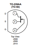
Representative J309 image (package may vary by manufacturer)