M66852FP
Overview
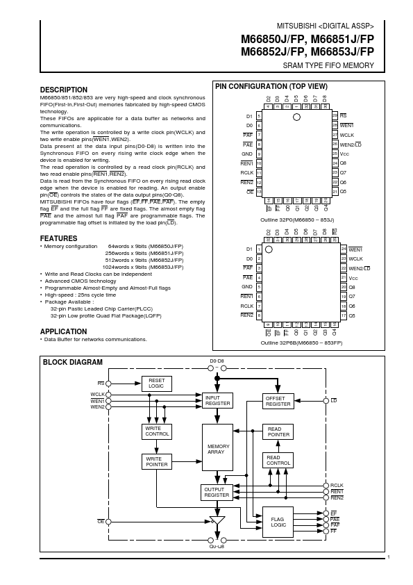
M66850/851/852/853 are very high-speed and clock synchronous FIFO(First-In,First-Out) memories fabricated by high-speed CMOS technology. These FIFOs are applicable for a data buffer as networks and communications.
- Memory configuration 64words x 9bits (M66850J/FP) 256words x 9bits (M66851J/FP) 512words x 9bits (M66852J/FP) 1024words x 9bits (M66853J/FP) Write and Read Clocks can be independent Advanced CMOS technology Programmable Almost-Empty and Almost-Full flags High-speed : 25ns cycle time Package Available : 32-pin Pastic Leaded Chip Carrier(PLCC) 32-pin Low profile Quad Flat Package(LQFP)