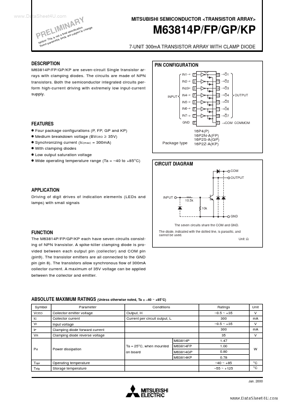
M63814P
M63814P is (M63814xx) 7-UNIT 300mA TRANSISTOR ARRAY manufactured by Mitsubishi Electric.
..
. . tion nge ifica to cha pec t al s subjec in f ot a are is n limits This ric ice: ramet t o N e pa Som
IM REL
RY A N I
MITSUBISHI SEMICONDUCTOR <TRANSISTOR ARRAY>
M63814P/FP/GP/KP
7-UNIT 300m A TRANSISTOR ARRAY WITH CLAMP DIODE
PIN CONFIGURATION
IN1→ IN2→ → INz3 INPUT IN4→ IN5→ IN6→ IN7→
1 2 3 4 5 6 7 8 16 →O1 15 →O2 14 →O3 13 →O4 12 →O5 11 →O6 10 →O7 9
DESCRIPTION M63814P/FP/GP/KP are seven-circuit Single transistor arrays with clamping diodes. The circuits are made of NPN transistors. Both the semiconductor integrated circuits perform high-current driving with extremely low input-current supply.
OUTPUT
Features q Four package configurations (P, FP, GP and KP) q Medium breakdown voltage (BVCEO ≥ 35V) q Synchronizing current (IC(max) = 300m A) q With clamping diodes q Low output saturation voltage q Wide operating temperature range (Ta =
- 40 to +85 °C)
→ MOM
Package type
16P4(P) 16P2N-A(FP) 16P2S-A(GP) 16P2Z-A(KP)
CIRCUIT DIAGRAM
OUTPUT
APPLICATION Driving of digit drives of indication elements (LEDs and lamps) with small signals
INPUT 10.5k 10k GND The seven circuits share the and GND.
FUNCTION The M63814P/FP/GP/KP each have seven circuits consisting of NPN transistor. A spike-killer clamping diode is provided between each output pin (collector) and pin (pin9). The transistor emitters are all connected to the GND pin (pin 8). The transistors allow synchronous flow of 300m A collector current. A maximum of 35V voltage can be applied between the collector and emitter.
The diode, indicated with the dotted line, is parasitic, and cannot be used. Unit:...