20N03HL
Overview
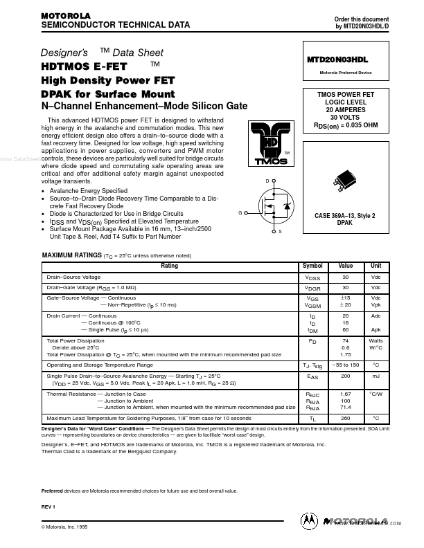
MOTOROLA SEMICONDUCTOR TECHNICAL DATA Order this document by MTD20N03HDL/D Designer's HDTMOS E-FET .™ High Density Power FET DPAK for Surface Mount N–Channel Enhancement–Mode Silicon Gate This adv...
| Part | 20N03HL |
|---|---|
| Description | MTD20N03HL |
| Manufacturer | Motorola Semiconductor |
| Size | 206.39 KB |
MOTOROLA SEMICONDUCTOR TECHNICAL DATA Order this document by MTD20N03HDL/D Designer's HDTMOS E-FET .™ High Density Power FET DPAK for Surface Mount N–Channel Enhancement–Mode Silicon Gate This adv...
| Part Number | Manufacturer | Description |
|---|---|---|
| 20N03L | Infineon | IPD20N03L |
| 20N03 | Inchange Semiconductor | N-Channel MOSFET |
| 20N06 | Inchange Semiconductor | N-Channel MOSFET |
| 20N06 | onsemi | N-Channel MOSFET |
| PSR-20N08A-JQ | MALLORY | Miniature Speaker |