Datasheet4U Logo Datasheet4U.com

MC1496B - BALANCED MODULATORS/DEMODULATORS

Download the MC1496B datasheet PDF. This datasheet also covers the MC1496 variant, as both devices belong to the same balanced modulators/demodulators family and are provided as variant models within a single manufacturer datasheet.

Features

  • upling and Bypass Capacitors Capacitors C1 and C2 (Figure 5) should be selected for a reactance of less than 5.0 Ω at the carrier frequency. Output Signal The output signal is taken from Pins 6 and 12 either balanced or single.
  • ended. Figure 11 shows the output levels of each of the two output sidebands resulting from variations in both the carrier and modulating signal inputs with a single.
  • ended output connection. Negative Supply VEE should be dc only. The insertion of an RF chok.

📥 Download Datasheet

Note: The manufacturer provides a single datasheet file (MC1496_Motorola.pdf) that lists specifications for multiple related part numbers.

Full PDF Text Transcription (Reference)

The following content is an automatically extracted verbatim text from the original manufacturer datasheet and is provided for reference purposes only.

View original datasheet text
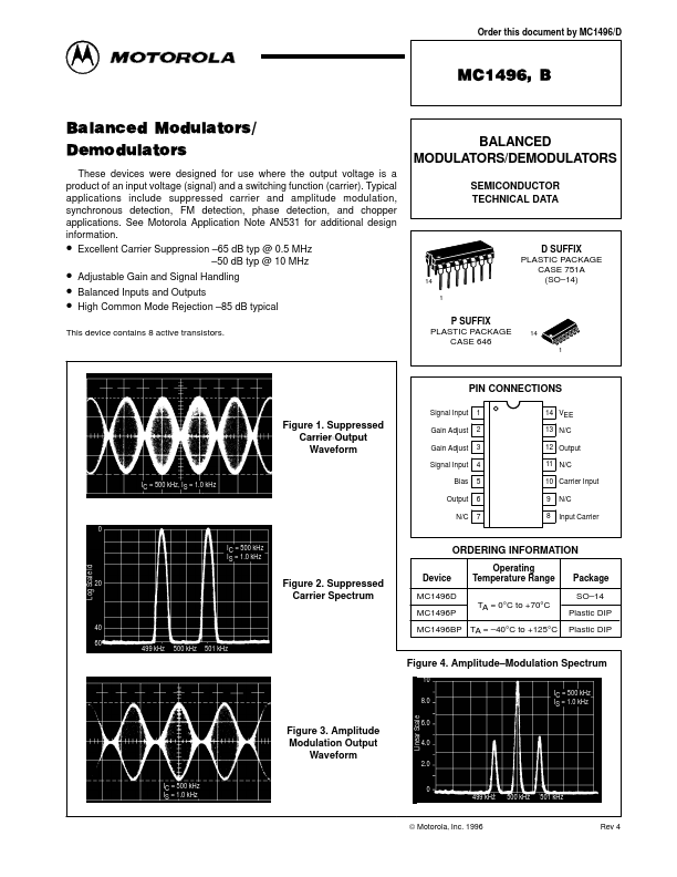
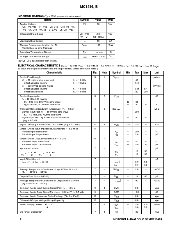
Order this document by MC1496/D MC1496, B Balanced Modulators/ Demodulators These devices were designed for use where the output voltage is a product of an input voltage (signal) and a switching function (carrier). Typical applications include suppressed carrier and amplitude modulation, synchronous detection, FM detection, phase detection, and chopper applications. See Motorola Application Note AN531 for additional design information. • Excellent Carrier Suppression –65 dB typ @ 0.
Published: |