Download MC33989 Datasheet PDF
Motorola Semiconductor
MC33989
MC33989 is System Basis Chip manufactured by Motorola Semiconductor.
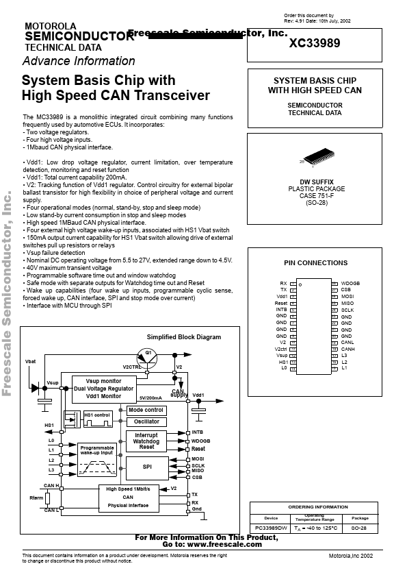
MOTOROLA Order this document by Rev: 4.91 Date: 10th July, 2002 Freescale Semiconductor, Inc. SEMICONDUCTOR TECHNICAL DATA XC33989 Advance Information System Basis Chip with High Speed CAN Transceiver The MC33989 is a monolithic integrated circuit bining many functions frequently used by automotive ECUs. It incorporates: - Two voltage regulators. - Four high voltage inputs. - 1Mbaud CAN physical interface. - Vdd1: Low drop voltage regulator, current limitation, over temperature detection, monitoring and reset function - Vdd1: Total current capability 200m A. - V2: Tracking function of Vdd1 regulator. Control circuitry for external bipolar ballast transistor for high flexibility in choice of peripheral voltage and current supply. - Four operational modes (normal, stand-by, stop and sleep mode) - Low stand-by current consumption in stop and sleep modes - High speed 1MBaud CAN physical interface. - Four external high voltage wake-up inputs, associated with HS1 Vbat switch - 150m A output current capability for HS1 Vbat switch allowing drive of external switches pull up resistors or relays - Vsup failure detection - Nominal DC operating voltage from 5.5 to 27V, extended range down to 4.5V. - 40V maximum transient voltage - Programmable software time out and window watchdog - Safe mode with separate outputs for Watchdog time out and Reset - Wake up capabilities (four wake up inputs, programmable cyclic sense, forced wake up, CAN interface, SPI and stop mode over current) - Interface with MCU through SPI SYSTEM BASIS CHIP WITH HIGH SPEED CAN SEMICONDUCTOR TECHNICAL DATA Freescale Semiconductor, Inc... DW SUFFIX PLASTIC PACKAGE CASE 751-F (SO-28) PIN CONNECTIONS RX TX Vdd1 Reset INTB GND GND GND GND V2 V2ctrl Vsup HS1 L0 1 2 3 4 5 6 7 8 9 10 11 12 13 14 28 27 26 25 24 23 22 21 20 19 18 17 16 15 Simplified Block Diagram Q1 Vbat V2CTRL Vsup V2 WDOGB CSB MOSI MISO SCLK GND GND GND GND CANL CANH L3 L2 L1 Vsup monitor Dual Voltage Regulator Vdd1 Monitor HS1...