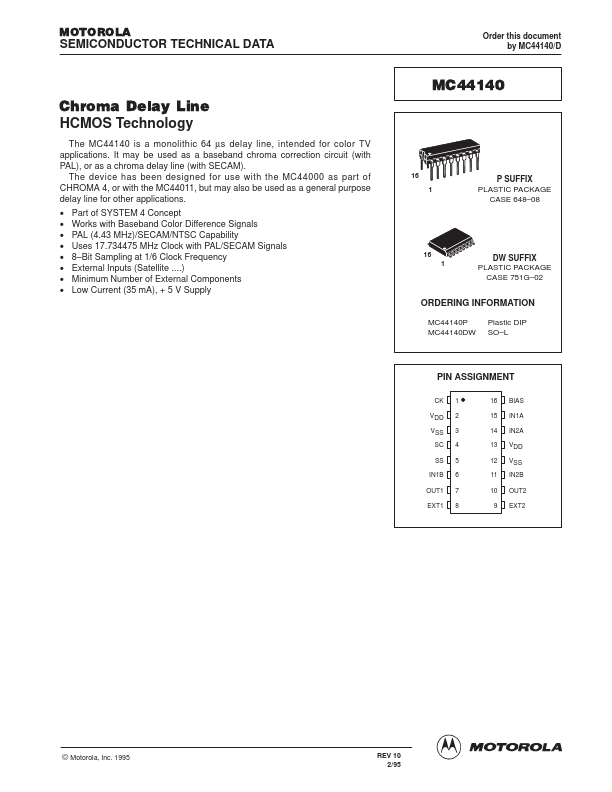
MC44140
Key Features
- Part of SYSTEM 4 Concept Works with Baseband Color Difference Signals PAL (4.43 MHz)/SECAM/NTSC Capability Uses 17.734475 MHz Clock with PAL/SECAM Signals 8
- Bit Sampling at 1/6 Clock Frequency External Inputs (Satellite ....) Minimum Number of External Components Low Current (35 mA), + 5 V Supply