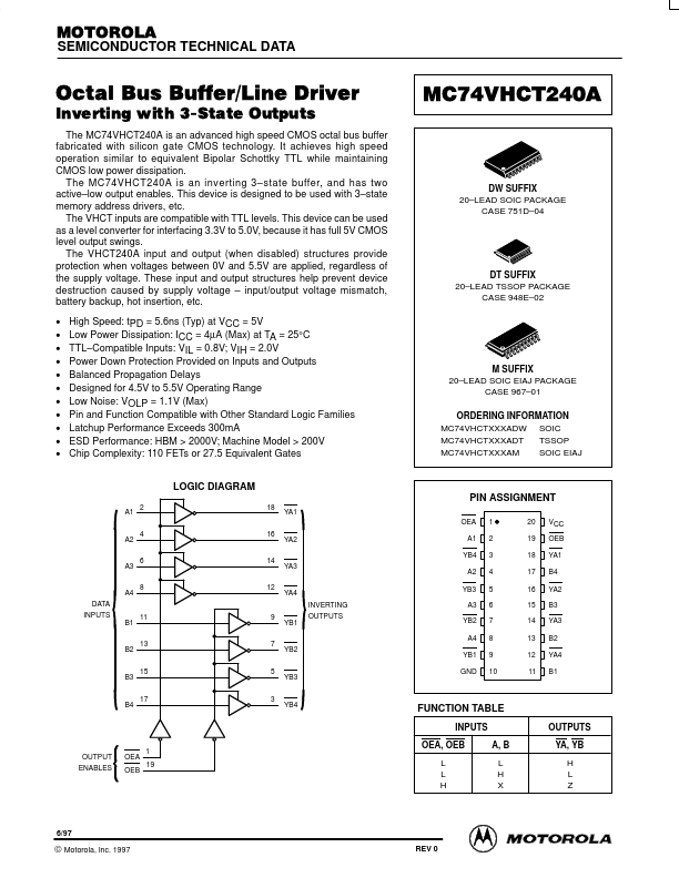
MC74VHCT240A
ÎÎÎÎÎÎÎÎÎÎÎÎÎÎÎÎÎÎÎÎÎÎÎMAXIMUM RATINGS*
ÎÎÎÎÎÎÎÎÎÎÎÎÎÎÎÎÎÎÎÎÎÎÎSymbol
Parameter
Value
Unit
ÎÎÎÎÎÎÎÎÎÎÎÎÎÎÎÎÎÎÎÎÎÎÎVCC
ÎÎÎÎÎÎÎÎÎÎÎÎÎÎÎÎÎÎÎÎÎÎÎVin
ÎÎÎÎÎÎÎÎÎÎÎÎÎÎÎÎÎÎÎÎÎÎÎÎÎÎÎÎÎÎÎÎÎÎÎÎÎÎÎÎÎÎÎÎÎÎVout
DC Supply Voltage
DC Input Voltage
DC Output Voltage
– 0.5 to + 7.0
– 0.5 to + 7.0
Output in 3–State – 0.5 to + 7.0
High or Low State – 0.5 to VCC + 0.5
V
V
V
ÎÎÎÎÎÎÎÎÎÎÎÎÎÎÎÎÎÎÎÎÎÎÎIIK Input Diode Current
ÎÎÎÎÎÎÎÎÎÎÎÎÎÎÎÎÎÎÎÎÎÎÎIOK Output Diode Current (VOUT < GND; VOUT > VCC)
ÎÎÎÎÎÎÎÎÎÎÎÎÎÎÎÎÎÎÎÎÎÎÎIout DC Output Current, per Pin
ÎÎÎÎÎÎÎÎÎÎÎÎÎÎÎÎÎÎÎÎÎÎÎICC DC Supply Current, VCC and GND Pins
ÎÎÎÎÎÎÎÎÎÎÎÎÎÎÎÎÎÎÎÎÎÎÎPD Power Dissipation in Still Air,
SOIC Packages†
TSSOP Package†
– 20
± 20
± 25
± 75
500
450
mA
mA
mA
mA
mW
ÎÎÎÎÎÎÎÎÎÎÎÎÎÎÎÎÎÎÎÎÎÎÎTstg Storage Temperature
– 65 to + 150
_C
ÎÎÎÎÎÎÎÎÎÎÎÎÎÎÎÎÎÎÎÎÎÎÎÎÎÎÎÎÎÎÎÎÎÎÎÎÎÎÎÎÎÎÎÎÎÎ* Absolute maximum continuous ratings are those values beyond which damage to the device
may occur. Exposure to these conditions or conditions beyond those indicated may adversely
affect device reliability. Functional operation under absolute–maximum–rated conditions is not
implied.
†Derating — SOIC Packages: – 7 mW/_C from 65_ to 125_C
TSSOP Package: – 6.1 mW/_C from 65_ to 125_C
This device contains protection
circuitry to guard against damage
due to high static voltages or electric
fields. However, precautions must
be taken to avoid applications of any
voltage higher than maximum rated
voltages to this high–impedance cir-
cuit. For proper operation, Vin and
v vVout should be constrained to the
range GND (Vin or Vout) VCC.
Unused inputs must always be
tied to an appropriate logic voltage
level (e.g., either GND or VCC).
Unused outputs must be left open.
RECOMMENDED OPERATING CONDITIONS
ÎÎÎÎÎÎÎÎÎÎÎÎÎÎÎÎÎÎÎÎÎÎÎSymbol
Parameter
Min Max Unit
ÎÎÎÎÎÎÎÎÎÎÎÎÎÎÎÎÎÎÎÎÎÎÎVCC DC Supply Voltage
4.5 5.5 V
ÎÎÎÎÎÎÎÎÎÎÎÎÎÎÎÎÎÎÎÎÎÎÎVin DC Input Voltage
ÎÎÎÎÎÎÎÎÎÎÎÎÎÎÎÎÎÎÎÎÎÎÎÎÎÎÎÎÎÎÎÎÎÎÎÎÎÎÎÎÎÎÎÎÎÎVout DCOutputVoltage
Output in 3–State
High or Low State
0
0
0
5.5
5.5
VCC
V
V
ÎÎÎÎÎÎÎÎÎÎÎÎÎÎÎÎÎÎÎÎÎÎÎTA Operating Temperature
ÎÎÎÎÎÎÎÎÎÎÎÎÎÎÎÎÎÎÎÎÎÎÎtr, tf Input Rise and Fall Time
– 40 + 85 _C
VCC =5.0V ±0.5V 0
20 ns/V
ÎÎÎÎÎÎÎÎÎÎÎÎÎÎÎÎÎÎÎÎÎÎÎDC ELECTRICAL CHARACTERISTICS
ÎÎÎÎÎÎÎÎÎÎÎÎÎÎÎÎÎÎÎÎÎÎÎÎÎÎÎÎÎÎÎÎÎÎÎÎÎÎÎÎÎÎÎÎÎÎÎÎÎÎÎÎÎÎÎÎÎÎÎÎÎÎÎÎÎÎSymbol
ÎÎÎÎÎÎÎÎÎÎÎÎÎÎÎÎÎÎÎÎÎÎÎÎÎÎÎÎÎÎÎÎÎVIH
ÎÎÎÎÎÎÎÎÎÎÎÎÎÎÎÎÎÎÎÎÎÎÎÎÎÎÎÎÎÎÎÎÎÎÎÎÎÎÎÎÎÎÎÎÎÎÎÎÎÎÎÎÎÎÎÎÎÎÎÎÎÎÎÎÎÎVIL
ÎÎÎÎÎÎÎÎÎÎÎÎÎÎÎÎÎÎÎÎÎÎÎÎÎÎÎÎÎÎÎÎÎÎÎÎÎÎÎÎÎÎÎÎÎÎÎÎÎÎÎÎÎÎÎÎÎÎÎÎÎÎÎÎÎÎVOH
ÎÎÎÎÎÎÎÎÎÎÎÎÎÎÎÎÎÎÎÎÎÎÎÎÎÎÎÎÎÎÎÎÎÎÎÎÎÎÎÎÎÎÎÎÎÎÎÎÎÎÎÎÎÎÎÎÎÎÎÎÎÎÎÎÎÎVOL
ÎÎÎÎÎÎÎÎÎÎÎÎÎÎÎÎÎÎÎÎÎÎÎÎÎÎÎÎÎÎÎÎÎÎÎÎÎÎÎÎÎÎÎÎÎÎÎÎÎÎÎÎÎÎÎÎÎÎÎÎÎÎÎÎÎÎÎÎÎÎÎÎÎÎÎÎÎÎÎÎÎÎÎÎÎÎÎÎÎÎÎÎÎÎÎÎÎÎÎIin
ÎÎÎÎÎÎÎÎÎÎÎÎÎÎÎÎÎÎÎÎÎÎÎÎÎÎÎÎÎÎÎÎÎIOZ
ÎÎÎÎÎÎÎÎÎÎÎÎÎÎÎÎÎÎÎÎÎÎÎÎÎÎÎÎÎÎÎÎÎÎÎÎÎÎÎÎÎÎÎÎÎÎÎÎÎÎÎÎÎÎÎÎÎÎÎÎÎÎÎÎÎÎÎÎÎÎÎÎÎÎÎÎÎÎÎÎÎÎÎÎÎÎÎÎÎÎÎÎÎÎÎÎÎÎÎÎÎÎÎÎÎÎÎÎÎÎÎÎÎÎÎÎÎÎÎÎÎÎÎÎÎÎÎÎÎÎÎÎICC
Parameter
Minimum High–Level
Input Voltage
Maximum Low–Level
Input Voltage
Minimum High–Level
Output Voltage
Vin = VIH or VIL
Maximum Low–Level
Output Voltage
Vin = VIH or VIL
Maximum Input
Leakage Current
Maximum 3–State
Leakage Current
Maximum Quiescent
Supply Current
Test Conditions
VCC
V
4.5 to
5.5
4.5 to
5.5
IOH = – 50µA 4.5
IOH = – 8mA 4.5
IOL = 50µA 4.5
IOL = 8mA 4.5
Vin = 5.5 V or GND
0 to 5.5
Vin = VIL or VIH
Vout = VCC or GND
Vin = VCC or GND
5.5
5.5
TA = 25°C
Min Typ Max
2.0
0.8
4.4 4.5
3.94
0.0 0.1
0.36
± 0.1
± 0.25
4.0
TA = – 40 to 85°C
Min Max
2.0
Unit
V
0.8 V
4.4 V
3.80
0.1 V
0.44
± 1.0
µA
± 2.5
µA
40.0 µA
MOTOROLA
2 VHC Data – Advanced CMOS Logic
DL203 — Rev 1