Click to expand full text
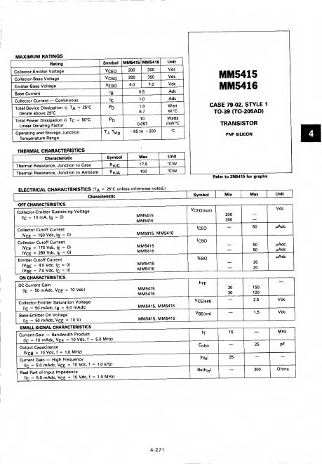
MAXIMUM RATINGS
Rating
Collector-Emitter Voltage
Collector-Base Voltage
Emitter-Base Voltage
Base Current
—Collector Current Continuous
@Total Device Dissipation T/ = 25°C
Derate above 25°C Total Power Dissipation (a Tc = 50°C
Linear Derating Factor Operating and Storage Junction
Temperature Range
Symbol MM5415 MM5416
v CEO VCBO VEBO
•b
"C
PD
200 300 200 350 4.0 7.0
0.5 1.0 1.0 6.7
Pd TJ- Tstg
10 0.057
- 65 to + 200
Unit
Vdc Vdc Vdc Adc Adc
Watt W/°C Watts mW/°C
,
MM5415 MM5416
CASE 79-02, STYLE 1
TO-39 (TO-205AD)
TRANSISTOR
PNP SILICON
Characteristic Thermal Resistance, Junction to Case
Thermal Resistance, Junction to Ambient
Symbol R&jc
RflJA
Max
17.5 150
Unit °C/W °c/w
I
Refer to 2N5415 for graphs.
ELECTRICAL CHARACTERISTICS (TA = 25°C unless otherwise noted.