MPC9449 Description
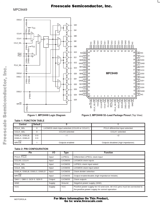
The MPC9449 is specifically designed to distribute LVCMOS patible clock signals up to a frequency of 200 MHz. The device has 15 identical outputs, organized in 4 output banks. Each output bank provides a retimed or frequency divided copy of the input signal with a near zero skew.
MPC9449 Key Features
- 15 LVCMOS patible clock outputs
- Two selectable LVCMOS and one differential LVPECL patible clock