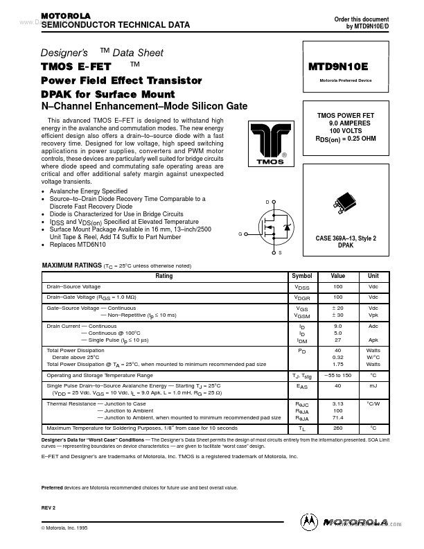
MTD9N10E Overview
Key Specifications
Package: DPAK
Pins: 3
Max Operating Temp: 150 °C
Min Operating Temp: -55 °C
Key Features
- Channel Enhancement
- Mode Silicon Gate
| Part | MTD9N10E |
|---|---|
| Description | TMOS POWER FET |
| Manufacturer | Motorola Semiconductor |
| Size | 207.99 KB |
Package: DPAK
Pins: 3
Max Operating Temp: 150 °C
Min Operating Temp: -55 °C
| Seller | Inventory | Price Breaks | Buy |
|---|---|---|---|
| Rochester Electronics | 30 | 100+ : 0.1718 USD 500+ : 0.1546 USD 1000+ : 0.1426 USD 10000+ : 0.1271 USD |
View Offer |
| Win Source | 5 | 45+ : 1.4081 USD 100+ : 1.1554 USD 155+ : 1.1193 USD 215+ : 1.0832 USD |
View Offer |
| Part Number | Manufacturer | Description |
|---|---|---|
| MTD9N10E | onsemi | Power MOSFET |