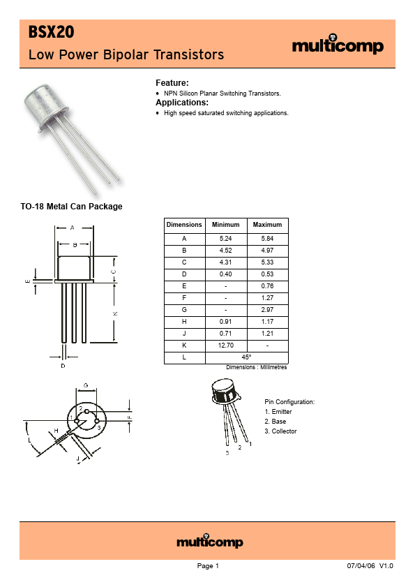
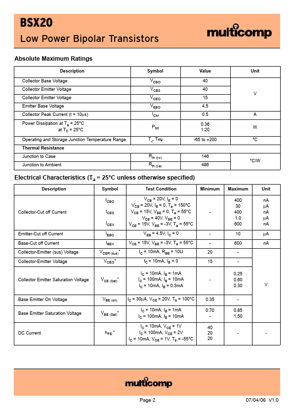
Collector Base Voltage Collector Emitter Voltage Collector Emitter Voltage Emitter Base Voltage Collector Peak Current (t = 10µs) Power Dissipation at Ta = 25°C
at TC = 25°C Operating and Storage Junction Temperature Range Thermal Resistance Junction to Case Junction to Ambient
Symbol VCBO VCES VCE
The following content is an automatically extracted verbatim text
from the original manufacturer datasheet and is provided for reference purposes only.
View original datasheet text
BSX20
Low Power Bipolar Transistors
Feature:
• NPN Silicon Planar Switching Transistors.
Applications:
• High speed saturated switching applications.
TO-18 Metal Can Package
Dimensions
A B C D E F G H J K L
Minimum Maximum
5.24 5.84
4.52 4.97
4.31 5.33
0.40 0.53
- 0.76
- 1.27
- 2.97
0.91 1.17
0.71 1.21
12.70
-
45° Dimensions : Millimetres
Pin Configuration: 1. Emitter 2. Base 3. Collector
Page 1
07/04/06 V1.