NCE80R1K2I
Description
The series of devices use advanced super junction technology and design to provide excellent RDS(ON) with low gate charge.
Key Features
- New technology for high voltage device
- Low on-resistance and low conduction losses
- Small package
- Ultra Low Gate Charge cause lower driving requirements
- 100% Avalanche Tested
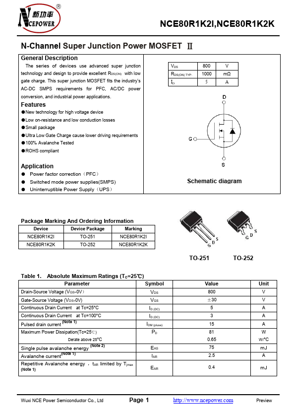
- ROHS pliant VDS RDS(ON) TYP。 ID 800 1000 5 V mΩ A