Datasheet4U Logo Datasheet4U.com

2SK2140-Z - N-Channel Power MOSFET

Download the 2SK2140-Z datasheet PDF. This datasheet also covers the 2SK2140 variant, as both devices belong to the same n-channel power mosfet family and are provided as variant models within a single manufacturer datasheet.

General Description

Transistor designed for high voltage switching applications.

Key Features

  • Low On-state Resistance RDS(on) = 1.5 Ω MAX. (VGS = 10 V, ID = 3.5 A).
  • Low Ciss Ciss = 930 pF TYP.
  • High Avalanche Capability Ratings.

📥 Download Datasheet

Note: The manufacturer provides a single datasheet file (2SK2140-NEC.pdf) that lists specifications for multiple related part numbers.

Full PDF Text Transcription for 2SK2140-Z (Reference)

Note: Below is a high-fidelity text extraction (approx. 800 characters) for 2SK2140-Z. For precise diagrams, and layout, please refer to the original PDF.

DATA SHEET MOS FIELD EFFECT TRANSISTOR 2SK2140, 2SK2140-Z SWITCHING N-CHANNEL POWER MOS FET INDUSTRIAL USE DESCRIPTION The 2SK2140, 2SK2140-Z is N-channel Power MOS Field...

View more extracted text
AL USE DESCRIPTION 
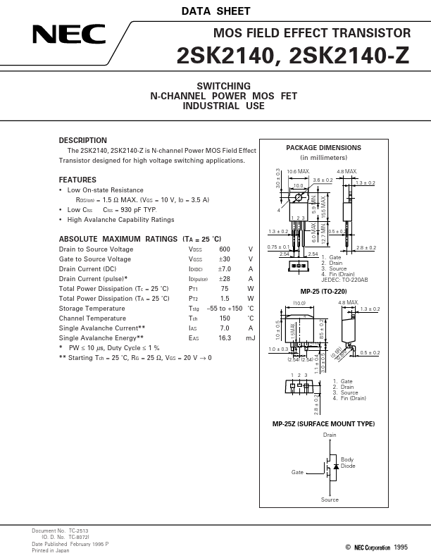
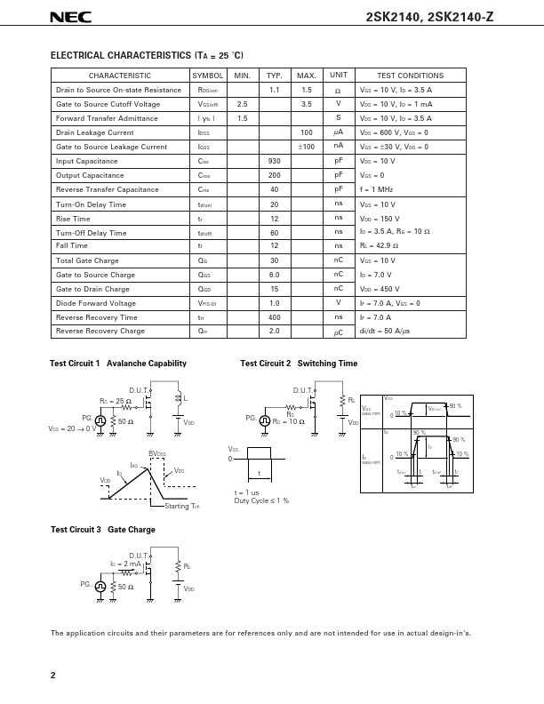
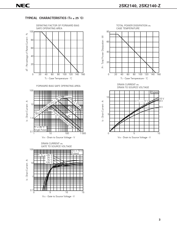
The 2SK2140, 2SK2140-Z is N-channel Power MOS Field Effect Transistor designed for high voltage switching applications. FEATURES • Low On-state Resistance RDS(on) = 1.5 Ω MAX. (VGS = 10 V, ID = 3.5 A) • Low Ciss Ciss = 930 pF TYP. • High Avalanche Capability Ratings ABSOLUTE MAXIMUM RATINGS (TA = 25 ˚C) Drain to Source Voltage VDSS 600 V Gate to Source Voltage VGSS ±30 V Drain Current (DC) ID(DC) ±7.0 A Drain Current (pulse)* ID(pulse) ±28 A Total Power Dissipation (Tc = 25 ˚C) PT1 75 W Total Power Dissipation (TA = 25 ˚C) PT2 1.5 W Storage Temperature Tstg –55 to +150 ˚C Channel Temperature Tch 150 ˚C S