UPA2450B
UPA2450B is N-Channel MOSFET manufactured by NEC.
DESCRIPTION
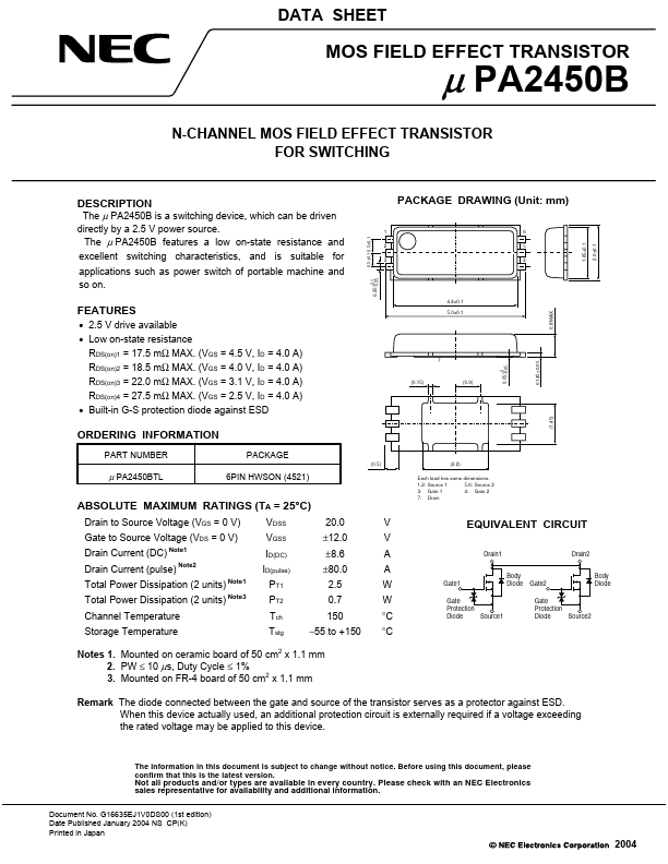
The µ PA2450B is a switching device, which can be driven directly by a 2.5 V power source. The µ PA2450B features a low on-state resistance and excellent switching characteristics, and is suitable for applications such as power switch of portable machine and so on.
1.85±0.1 0.145±0.05 (1.45) 0.8 MAX.
2 3
5 4
0.25 +0.1 -0.05
4.4±0.1
FEATURES
- 2.5 V drive available
- Low on-state resistance RDS(on)1 = 17.5 mΩ MAX. (VGS = 4.5 V, ID = 4.0 A) RDS(on)2 = 18.5 mΩ MAX. (VGS = 4.0 V, ID = 4.0 A) RDS(on)3 = 22.0 mΩ MAX. (VGS = 3.1 V, ID = 4.0 A) RDS(on)4 = 27.5 mΩ MAX. (VGS = 2.5 V, ID = 4.0 A)
- Built-in G-S protection diode against ESD
5.0±0.1
0.05 +0 -0.05
(0.15)
(0.9)
ORDERING INFORMATION
PART NUMBER PACKAGE
(0.5) (2.2) Each lead has same dimensions. 5,6: Source 2 1,2: Source 1 4: Gate 2 3: Gate 1 7: Drain
µ PA2450BTL
6PIN HWSON (4521)
ABSOLUTE MAXIMUM RATINGS (TA = 25°C)
Drain to Source Voltage (VGS = 0 V) Gate to Source Voltage (VDS = 0 V) Drain Current (DC) Note1 Drain Current (pulse)
Note2 Note1
VDSS VGSS ID(DC) ID(pulse) PT1 PT2 Tch Tstg
20.0 ±12.0 ±8.6 ±80.0 2.5 0.7 150
- 55 to +150
V V A A W W °C °C
Gate1
EQUIVALENT CIRCUIT
Drain1 Drain2
Total Power Dissipation (2 units) Channel Temperature Storage Temperature
Body Diode
Gate2 Gate Protection Diode Source2
Total Power Dissipation (2 units) Note3
Gate Protection Diode Source1
Notes 1. Mounted on ceramic board of 50 cm2 x 1.1 mm 2. PW ≤ 10 µs, Duty Cycle ≤ 1% 2 3. Mounted on FR-4 board of 50 cm x 1.1 mm Remark The diode connected between the gate and source of the transistor serves as a protector against ESD. When this device actually used, an additional protection circuit is externally required if a voltage exceeding the rated voltage may be applied to this device.
The information in this document is subject to change without notice. Before using this document, please confirm that this is the latest version.
Not all products and/or types are available in every country....