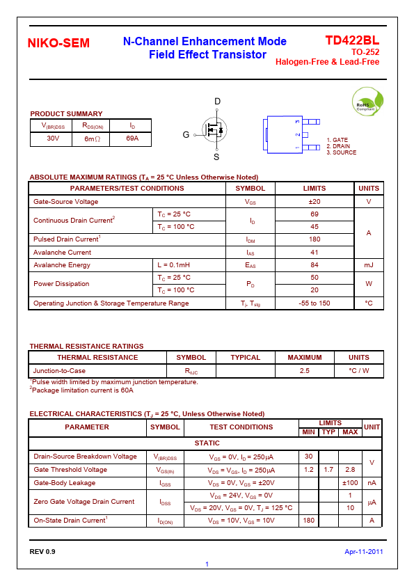
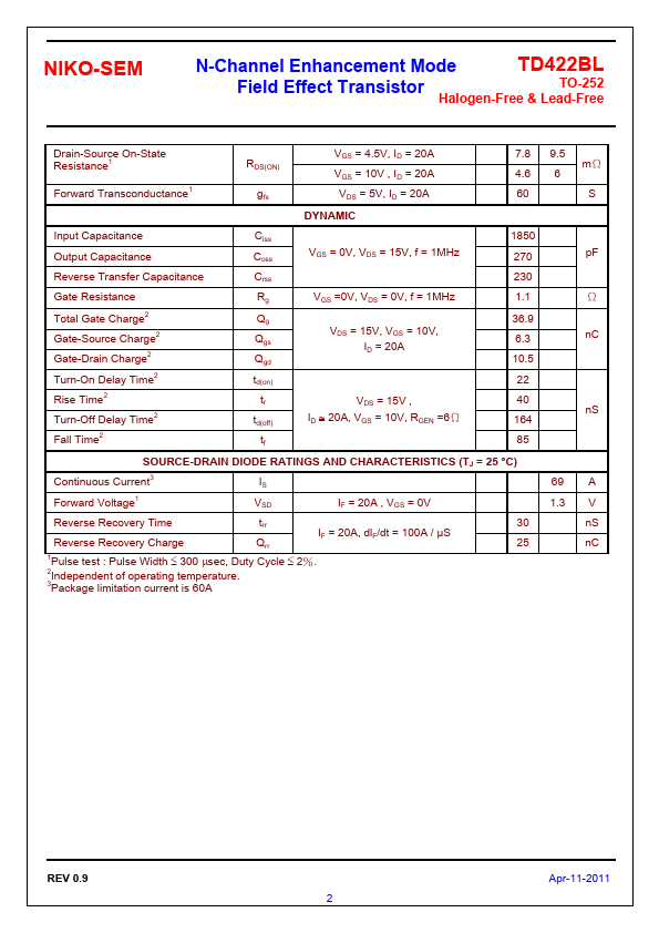
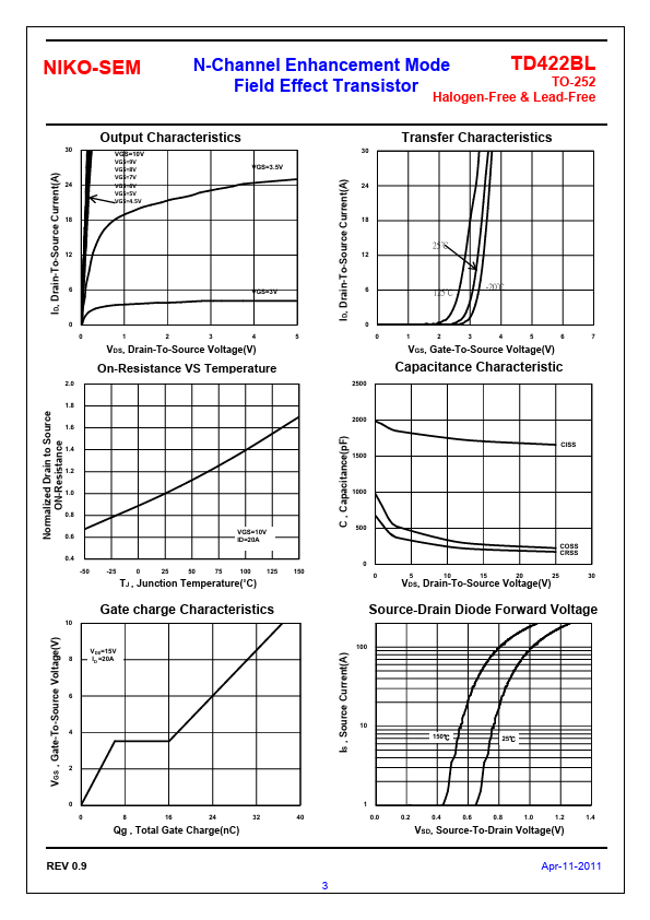
TD422BL Overview
Pulse Width 300 sec, Duty Cycle 2%. 2Independent of operating temperature.
TD422BL datasheet by NIKO-SEM.
This datasheet includes multiple variants, all published together in a single manufacturer document.
| Part number | TD422BL |
|---|---|
| Datasheet | TD422BL TD422BL-NIKO Datasheet (PDF) |
| File Size | 276.57 KB |
| Manufacturer | NIKO-SEM |
| Description | N-Channel Enhancement Mode Field Effect Transistor |
|
|
Pulse Width 300 sec, Duty Cycle 2%. 2Independent of operating temperature.
| Brand Logo | Part Number | Description | Other Manufacturers |
|---|---|---|---|
| TD422BL | N-Channel Enhancement Mode MOSFET | UNIKC |
| Part Number | Description |
|---|