NJM2507
NJM2507 is Video Differential Input Receiver manufactured by New Japan Radio.
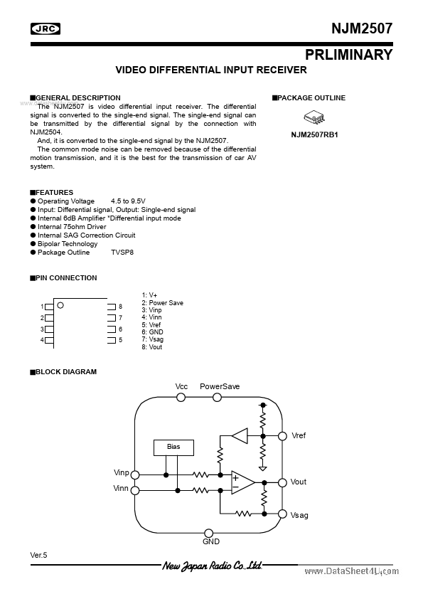
DESCRIPTION
The NJM2507 is video differential input receiver. The differential signal is converted to the single-end signal. The single-end signal can be transmitted by the differential signal by the connection with NJM2504. And, it is converted to the single-end signal by the NJM2507. The mon mode noise can be removed because of the differential motion transmission, and it is the best for the transmission of car AV system. QPACKAGE OUTLINE
..
NJM2507RB1
QFEATURES O Operating Voltage 4.5 to 9.5V O Input: Differential signal, Output: Single-end signal O Internal 6d B Amplifier
- Differential input mode O Internal 75ohm Driver O Internal SAG Correction Circuit O Bipolar Technology O Package Outline TVSP8
QPIN CONNECTION
1: V+ 2: Power Save 3: Vinp 4: Vinn 5: Vref 6: GND 7: Vsag 8: Vout
1 2 3 4
8 7 6 5
QBLOCK DIAGRAM
Vcc
Power Save
Vref
Bias
Vinp Vinn Vout
Vsag GND
Ver.5 -1-
QABSOLUTE MAXIMUM RATINGS(Ta=25°C) PARAMETER SYMBOL RATINGS UNIT + Supply Voltage V 10 V Power Dissipation P 580(Note1) m W D .. Operating Temperature Range Topr -40 to +85(Note2) °C Storage Temperature Range Tstg -40 to +150 °C (Note 1) At on a board of EIA/JEDEC specification. (114.3 x 76.2 x 1.6mm 2 layers, FR-4) (Note 2) It has high operating temperature range product.(-40 to +105°C) QRECENDED OPERATING CONDITIONS(Ta=25°C) PARAMETER Operating voltage SYMBOL Vopr TEST CONDITION MIN. 4.5 TYP. MAX. 9.0 UNIT V
QELECTRICAL CHRACTERISTCS( V+ =5V, RL=150ohm,Ta=25°C) PARAMETER Supply Current Supply Current at Power Save Mode Maximum Output Level Voltage Gain Frequency Characteristics mon Mode Rejection Ratio Differential Gain Differential Phase SW Voltage High Level SW Voltage Low Level SW Sink Current High Level SW Sink Current Low Level SYMBOL ICC Isave Vom Gv Gf CMR DG DP Vth H Vth L Ith H Ith L No signal Power save mode Vin=100k Hz,sin-signal, THD=1%, Vin=1MHz,1.0Vp-p sin-signal Vin=10MHz/1MHz, 1.0Vpp sin-signal Vin=20k Hz, 1.0Vpp,sin-signal Vin=1.0Vp-p 10step video signal Vin=1.0Vp-p...