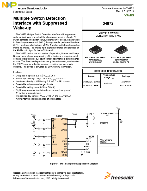
Datasheet4U Logo Datasheet4U.com

34972 Datasheet - NXP

Multiple Switch Detection Interface

34972 Features

* a 22-to-1 analog multiplexer for reading inputs as analog. The analog input signal is buffered and provided on the AMUX output pin for the MCU to read. The 34972 device has two modes of operation, Normal and Sleep. Normal mode allows programming of the device and supplies switch contacts with pull-u

34972 General Description

of each pin can be found in the Functional Pin Description section beginning on page 9. Table 1. 34972 Pin Definitions Pin Number Pin Name Pin Function Formal Name Definition 1 GND Ground 2 SI Input 3 SCLK Input 4 CS Input Ground SPI Slave In Serial Clock Chip Select Ground for log.

34972 Datasheet (1.75 MB)

Preview of 34972 PDF

Datasheet Details

Part number:

34972

Manufacturer:

NXP ↗

File Size:

1.75 MB

Description:

Multiple switch detection interface.
Freescale Semiconductor Technical Data Document Number: MC34972 Rev. 1.0, 9/2013 Multiple Switch Detection Interface with Suppressed Wake-up 34972.

📁 Related Datasheet

34978 22-channel multiple switch detection interface (NXP)

3490 Linear Low Density Polyethylene (TAISOX)

34901 High-speed CAN Transceiver (Freescale Semiconductor)

34903 System Basis Chip - SBC (Freescale Semiconductor)

34904 System Basis Chip - SBC (Freescale Semiconductor)

34905 System Basis Chip - SBC (Freescale Semiconductor)

34920 Quad H-Bridge Motor Driver (Freescale Semiconductor)

34921 Configurable Motor Driver IC (Freescale Semiconductor)

34923 Full-Bridge PWM Motor Driver (Freescale Semiconductor)

34931 5.0A H-Bridge (NXP)

TAGS

34972 Multiple Switch Detection Interface NXP

Image Gallery

34972 Datasheet Preview Page 2 34972 Datasheet Preview Page 3

34972 Distributor