Datasheet4U Logo Datasheet4U.com

74AUP1G79 - Low-power D-type flip-flop

Description

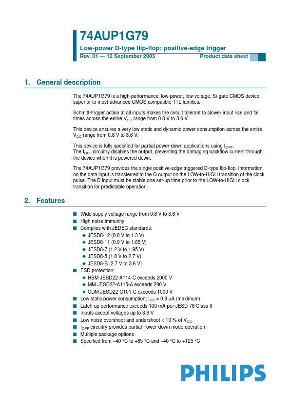
The 74AUP1G79 is a high-performance, low-power, low-voltage, Si-gate CMOS device, superior to most advanced CMOS compatible TTL families.

Schmitt-trigger action at all inputs makes the circuit tolerant to slower input rise and fall times across the entire VCC range from 0.8 V to 3.6 V.

Features

  • s Wide supply voltage range from 0.8 V to 3.6 V s High noise immunity s Complies with JEDEC standards: x JESD8-12 (0.8 V to 1.3 V) x JESD8-11 (0.9 V to 1.65 V) x JESD8-7 (1.2 V to 1.95 V) x JESD8-5 (1.8 V to 2.7 V) x JESD8-B (2.7 V to 3.6 V) s ESD protection: x HBM JESD22-A114-C exceeds 2000 V x MM JESD22-A115-A exceeds 200 V x CDM JESD22-C101-C exceeds 1000 V s Low static power consumption; ICC = 0.9 µA (maximum) s Latch-up performance exceeds 100 mA per JESD 78 Class II s Inputs accept voltage.

📥 Download Datasheet

Full PDF Text Transcription (Reference)

The following content is an automatically extracted verbatim text from the original manufacturer datasheet and is provided for reference purposes only.

View original datasheet text
www.DataSheet4U.com 74AUP1G79 Low-power D-type flip-flop; positive-edge trigger Rev. 01 — 12 September 2005 Product data sheet 1. General description The 74AUP1G79 is a high-performance, low-power, low-voltage, Si-gate CMOS device, superior to most advanced CMOS compatible TTL families. Schmitt-trigger action at all inputs makes the circuit tolerant to slower input rise and fall times across the entire VCC range from 0.8 V to 3.6 V. This device ensures a very low static and dynamic power consumption across the entire VCC range from 0.8 V to 3.6 V. This device is fully specified for partial power-down applications using IOFF. The IOFF circuitry disables the output, preventing the damaging backflow current through the device when it is powered down.
Published: |