Datasheet Details
| Part number | 74LVC1G14 |
|---|---|
| Manufacturer | NXP Semiconductors |
| File Size | 190.32 KB |
| Description | Single Schmitt-trigger inverter |
| Datasheet |
 74LVC1G14 Datasheet 74LVC1G14 Datasheet
|
|
|
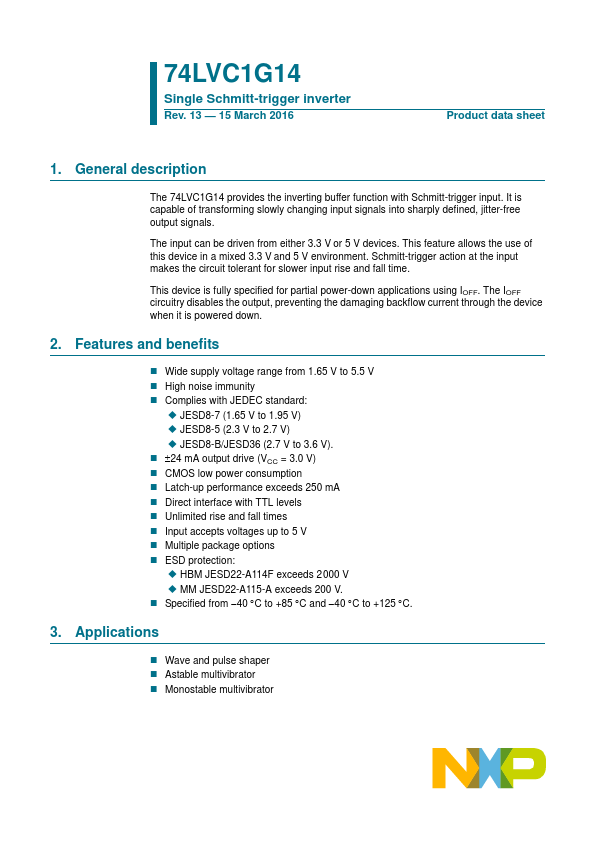
The 74LVC1G14 provides the inverting buffer function with Schmitt-trigger input.
It is capable of transforming slowly changing input signals into sharply defined, jitter-free output signals.
The input can be driven from either 3.3 V or 5 V devices.
| Part number | 74LVC1G14 |
|---|---|
| Manufacturer | NXP Semiconductors |
| File Size | 190.32 KB |
| Description | Single Schmitt-trigger inverter |
| Datasheet |
74LVC1G14 Datasheet
|
|
|
|