LPC3130 Description
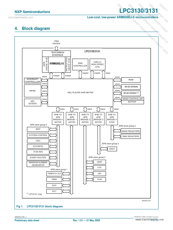
The NXP LPC3130/3131 bine an 180 MHz ARM926EJ-S CPU core, high-speed USB 2.0 On-The-Go (OTG), up to 192 KB SRAM, NAND flash controller, flexible external bus interface, four channel 10-bit ADC, and a myriad of serial and parallel interfaces in a single chip targeted at consumer, industrial, medical, and munication markets. To optimize system power consumption, the LPC3130/3131 have multiple power domains and a very...
LPC3130 Key Features
- CPU platform 180 MHz, 32-bit ARM926EJ-S 16 kB D-cache and 16 kB I-cache Memory Management Unit (MMU)
- Internal memory 96 kB (LPC3130) or 192 kB (LPC3131) embedded SRAM
- External memory interface NAND flash controller with 8-bit ECC 8/16-bit Multi-Port Memory Controller (MPMC): SDRAM a
- System functions Dynamic clock gating and scaling Multiple power domains Selectable boot-up: SPI flash, NAND flash
- Operating voltage and temperature Core voltage: 1.2 V I/O voltage: 1.8 V, 2.8 V, 3.3 V Temperature: -40 °C to +85
- TFBGA180 package: 12 × 12 mm2, 0.8 mm pitch