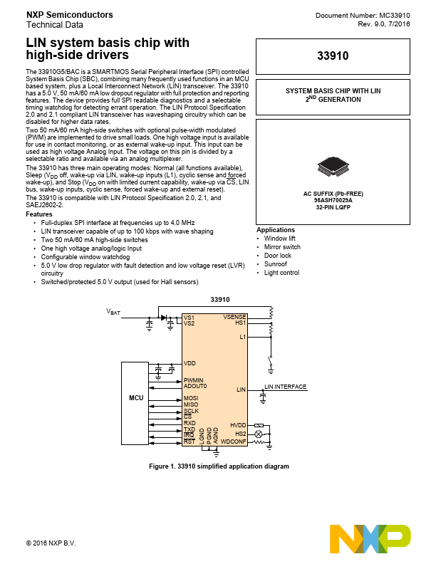
Datasheet4U Logo Datasheet4U.com

MC33910 - LIN transceiver

Datasheet Summary

Description

of each pin can be found in the Functional pin description.

Table 2.

This pin is the receiver output of the LIN interface which reports the state of the bus voltage to the MCU interface.

Features

  • The device provides full SPI readable diagnostics and a selectable timing watchdog for detecting errant operation. The LIN Protocol Specification 2.0 and 2.1 compliant LIN transceiver has waveshaping circuitry which can be disabled for higher data rates. Two 50 mA/60 mA high-side switches with optional pulse-width modulated (PWM) are implemented to drive small loads. One high voltage input is available for use in contact monitoring, or as external wake-up input. This input can be used as high v.

📥 Download Datasheet

Datasheet preview – MC33910

Datasheet Details

Part number MC33910
Manufacturer NXP
File Size 2.04 MB
Description LIN transceiver
Datasheet download datasheet MC33910 Datasheet
Additional preview pages of the MC33910 datasheet.
Other Datasheets by NXP

Full PDF Text Transcription

Click to expand full text
NXP Semiconductors Technical Data MC33910G5AC/MC3433910G5AC Document Number: MC33910 Rev. 9.0, 7/2016 LIN system basis chip with high-side drivers 33910 The 33910G5/BAC is a SMARTMOS Serial Peripheral Interface (SPI) controlled System Basis Chip (SBC), combining many frequently used functions in an MCU based system, plus a Local Interconnect Network (LIN) transceiver. The 33910 has a 5.0 V, 50 mA/60 mA low dropout regulator with full protection and reporting features. The device provides full SPI readable diagnostics and a selectable timing watchdog for detecting errant operation. The LIN Protocol Specification 2.0 and 2.1 compliant LIN transceiver has waveshaping circuitry which can be disabled for higher data rates.
Published: |