PRTR5V0U2F
PRTR5V0U2F is Ultra low capacitance double rail-to-rail ESD protection manufactured by NXP Semiconductors.
description
Ultra low capacitance double rail-to-rail Electro Static Discharge (ESD) protection devices in leadless ultra small Surface-Mounted Device (SMD) plastic packages.
The devices are designed to protect two Hi-Speed data lines or high-frequency signal lines from the damage caused by ESD and other transients.
PRTR5V0U2F and PRTR5V0U2K integrate two ultra low capacitance rail-to-rail ESD protection channels and one additional ESD protection diode each to ensure signal line protection even if no supply voltage is available.
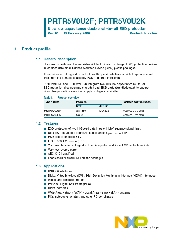
Table 1. Product overview
Type number
Package
SOT886
PRTR5V0U2K
SOT891
JEDEC MO-252
- Package configuration leadless ultra small leadless ultra small
1.2 Features
I ESD protection of two Hi-Speed data lines or high-frequency signal lines I Ultra low input/output to ground capacitance: C(I/O-GND) = 1 p F I ESD protection up to 8 k V I IEC 61000-4-2, level 4 (ESD) I Very low clamping voltage due to an integrated additional ESD protection diode I Very low reverse current I AEC-Q101 qualified I Leadless ultra small SMD plastic packages
1.3 Applications
I USB 2.0 interfaces I Digital Video Interface (DVI) / High Definition Multimedia Interface (HDMI) interfaces I Mobile and cordless phones I Personal Digital Assistants (PDA) I Digital cameras I Wide Area Network (WAN) / Local Area Network (LAN) systems I PCs, notebooks, printers and other PC peripherals
NXP Semiconductors
PRTR5V0U2F; PRTR5V0U2K
Ultra low capacitance double rail-to-rail ESD protection
1.4 Quick reference data
Table 2. Quick reference data Tamb = 25 °C unless otherwise specified.
Symbol Parameter
Per channel
C(I/O-GND) input/output to ground capacitance
C(I/O-I/O) input/output to input/output capacitance
Zener diode
VRWM Csup reverse standoff voltage supply pin to ground capacitance
[1] Measured from pin 1, 3, 4 or 6 to ground. [2] Measured from pin 1 or 6 to pin 3 or 4. [3] Measured from pin 5 to ground.
Conditions f = 1 MHz; V(I/O-GND) = 0 V f...