Datasheet Summary
..
NanoAmp Solutions, Inc. 1982 Zanker Road, San Jose, CA 95112 ph: 408-573-8878, FAX: 408-573-8877 .nanoamp.
Advance Information
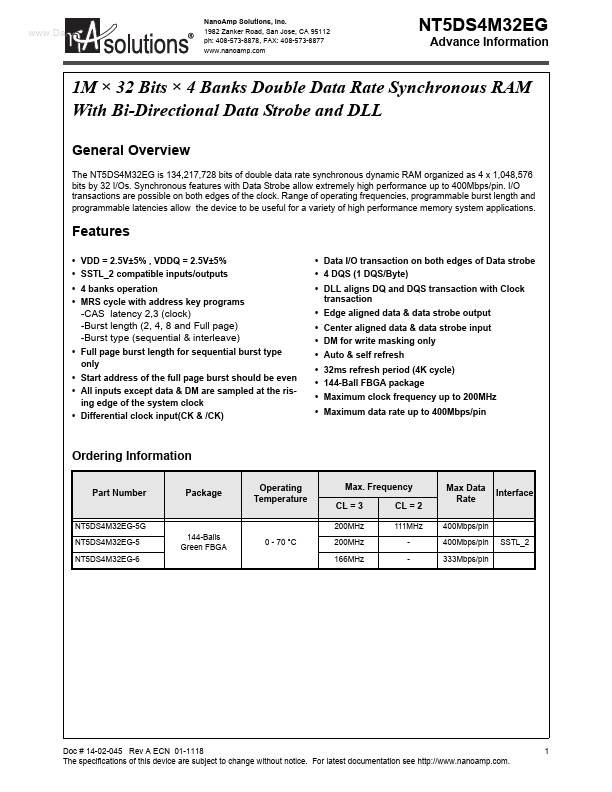
1M × 32 Bits × 4 Banks Double Data Rate Synchronous RAM With Bi-Directional Data Strobe and DLL
General Overview
The NT5DS4M32EG is 134,217,728 bits of double data rate synchronous dynamic RAM organized as 4 x 1,048,576 bits by 32 I/Os. Synchronous Features with Data Strobe allow extremely high performance up to 400Mbps/pin. I/O transactions are possible on both edges of the clock. Range of operating frequencies, programmable burst length and programmable latencies allow the device to be useful for a variety of high...


