Datasheet4U Logo Datasheet4U.com

M2N2G64TU8HG4B - Unbuffered DDR2 SO-DIMM

Download the M2N2G64TU8HG4B datasheet PDF. This datasheet also covers the M2N1G64TUH8G5F variant, as both devices belong to the same unbuffered ddr2 so-dimm family and are provided as variant models within a single manufacturer datasheet.

General Description

M2N1G64TUH8G5F / M2S1G64TUH8G4F / M2N2G64TU8HG5B / M2N2G64TU8HG4B are unbuffered 200-Pin Double Data Rate 2 (DDR2) Synchronous DRAM Small Outline Dual In-Line Memory Module (SO-DIMM), organized as two ranks of 128Mx64 (1GB)/256Mx64 (2GB) high-speed memory array.

Key Features

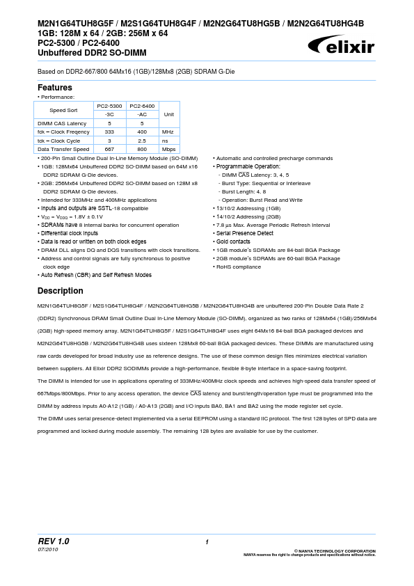
  • Performance: Speed Sort DIMM CAS Latency fck.
  • Clock Freqency tck.
  • Clock Cycle Data Transfer Speed PC2-5300 -3C 5 333 3 667 PC2-6400 -AC 5 400 2.5 800 MHz ns Mbps.
  • Automatic and controlled precharge commands.
  • Programmable Operation: - DIMM  Latency: 3, 4, 5 - Burst Type: Sequential or Interleave - Burst Length: 4, 8 - Operation: Burst Read and Write.
  • 13/10/2 Addressing (1GB).
  • 14/10/2 Addressing (2GB).
  • 7.8 s Max. Average.

📥 Download Datasheet

Note: The manufacturer provides a single datasheet file (M2N1G64TUH8G5F-Nanya.pdf) that lists specifications for multiple related part numbers.

Datasheet Details

Part number M2N2G64TU8HG4B
Manufacturer Nanya
File Size 364.08 KB
Description Unbuffered DDR2 SO-DIMM
Datasheet download datasheet M2N2G64TU8HG4B Datasheet

Full PDF Text Transcription (Reference)

The following content is an automatically extracted verbatim text from the original manufacturer datasheet and is provided for reference purposes only.

View original datasheet text
M2N1G64TUH8G5F / M2S1G64TUH8G4F / M2N2G64TU8HG5B / M2N2G64TU8HG4B 1GB: 128M x 64 / 2GB: 256M x 64 PC2-5300 / PC2-6400 Unbuffered DDR2 SO-DIMM Based on DDR2-667/800 64Mx16 (1GB)/128Mx8 (2GB) SDRAM G-Die Features • Performance: Speed Sort DIMM CAS Latency fck – Clock Freqency tck – Clock Cycle Data Transfer Speed PC2-5300 -3C 5 333 3 667 PC2-6400 -AC 5 400 2.5 800 MHz ns Mbps • Automatic and controlled precharge commands • Programmable Operation: - DIMM  Latency: 3, 4, 5 - Burst Type: Sequential or Interleave - Burst Length: 4, 8 - Operation: Burst Read and Write • 13/10/2 Addressing (1GB) • 14/10/2 Addressing (2GB) • 7.8 s Max.