NT5DS64M4AT
NT5DS64M4AT is (NT5DSxxMxAx) 256Mb DDR333/300 SDRAM manufactured by Nanya.
- Part of the NT5DS32M8AT comparator family.
- Part of the NT5DS32M8AT comparator family.
..
NT5DS64M4AT NT5DS64M4AW NT5DS32M8AT NT5DS32M8AW
256Mb DDR333/300 SDRAM Features
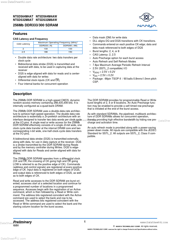
CAS Latency and Frequency
CAS Latency 2 2.5 Maximum Operating Frequency (MHz)- DDR333 (-6) DDR300 (-66) 133 133 166 150
- Double data rate architecture: two data transfers per clock cycle
- Bidirectional data strobe (DQS) is transmitted and received with data, to be used in capturing data at the receiver
- DQS is edge-aligned with data for reads and is centeraligned with data for writes
- Differential clock inputs (CK and CK)
- Four internal banks for concurrent operation
- Data mask (DM) for write data
- DLL aligns DQ and DQS transitions with CK transitions.
- mands entered on each...