NT5TU64M16HZ Description
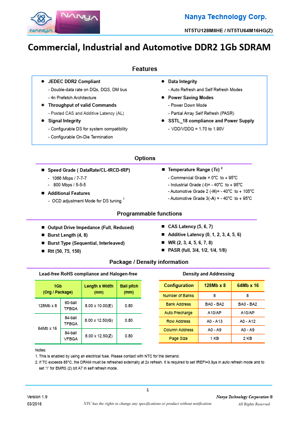
D1GDbR2D1DGRb2 SDRAM H-Die NT5TU128M8HE / NT5TU64M16HG(Z) Nanya Technology Corp. NT5TU128M8HE / NT5TU64M16HG(Z) mercial, Industrial and Automotive DDR2 1Gb SDRAM.
NT5TU64M16HZ Key Features
- JEDEC DDR2 pliant
- Double-data rate on DQs, DQS, DM bus
- 4n Prefetch Architecture
- Throughput of valid mands
- Posted CAS and Additive Latency (AL)
- Signal Integrity
- Configurable DS for system patibility
- Configurable On-Die Termination
- Data Integrity
- Auto Refresh and Self Refresh Modes


