74F283
74F283 is 4-Bit Binary Full Adder manufactured by National.
54F 74F283 4-Bit Binary Full Adder with Fast Carry
November 1994
54F 74F283 4-Bit Binary Full Adder with Fast Carry
General Description
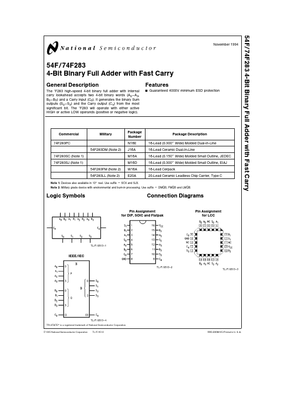
The ’F283 high-speed 4-bit binary full adder with internal carry lookahead accepts two 4-bit binary words (A0
- A3 B0
- B3) and a Carry input (C0) It generates the binary Sum outputs (S0
- S3) and the Carry output (C4) from the most significant bit The ’F283 will operate with either active HIGH or active LOW operands (positive or negative logic)
Features
Guaranteed 4000V minimum ESD protection mercial 74F283PC
Military
Package Number N16E
Package Description 16-Lead (0 300 Wide) Molded Dual-In-Line 16-Lead Ceramic Dual-In-Line 16-Lead (0 150...