2N5518 Overview
Description
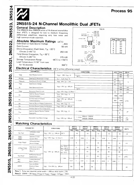
The 2N5515 thru 2N5524 series of N-channel monolithic dual JFETs is designed for low to medium frequency differential amplifiers requiring very low noise and high common-mode rejection. Gate-Drain or Gate-Source Voltage -40V Gate Current 50 mA Device Dissipation (Each Side), Ta = 85°C (Derate 2 mW/°C) 250 mW Total Device Dissipation, T/\ = 85°C (Derate 3 mW/°C) 375 mW Storage Temperature Range Lead Temperature (1/16" from case -65°Cto+150°C for 10 seconds) 300° C Dual JFETs n„ ' I mum .016-11.1119 * "lie"- -o.4i3i ddo) PARAMETER CONDITIONS IGSS BV GSS v GS(off) VGS lG Gate Reverse Current Gate-Source Breakdown Voltage Gate-Source Cutoff Voltage Gate-Source Voltage Gate Operating Current V GS = -30V, V DS ^Q lG = 1 /J A, V DS = VDS- 20V, Dl = 1 nA V D G = 20V, Dl = 200 /iA 150"C PIN FET (12) 1 SI 2 D1 3 G1 5 S2 6 D2 7 G2 MIN MAX -250 PA -250 nA -40 -0,7 -4 V -0.2 -3.8 -100 PA IDSS 9fs yos 9os Cjss Saturation Drain Current Common-Source Forward Common-Source Forward Transconductance Common -Sou ret' Output Conductance Common-Source Output Conductance Common-Source Input Capacitance Common-Source Reverse Transfer Capacitance V DS =20V.